

XCV100-5BG256I
Product Overview
Category
The XCV100-5BG256I belongs to the category of Field Programmable Gate Arrays (FPGAs).
Use
FPGAs are integrated circuits that can be programmed and reprogrammed to perform various digital functions. The XCV100-5BG256I is specifically designed for applications requiring high-performance logic and digital signal processing.
Characteristics
- High-performance FPGA with advanced features
- Flexible and reprogrammable design
- Suitable for complex digital designs
- Offers a wide range of I/O options
- Low power consumption
- Reliable and durable
Package
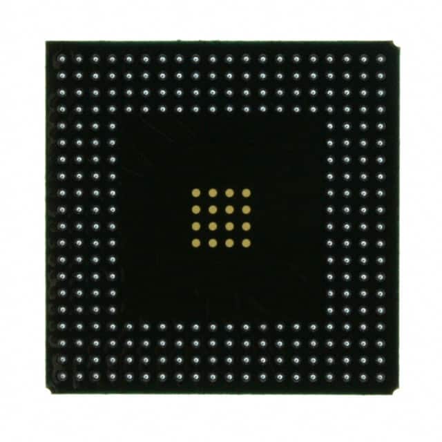
The XCV100-5BG256I comes in a 256-ball grid array (BGA) package, which provides a compact and reliable form factor for easy integration into electronic systems.
Essence
The essence of the XCV100-5BG256I lies in its ability to provide customizable digital logic functionality, allowing designers to implement complex algorithms and processing tasks efficiently.
Packaging/Quantity
The XCV100-5BG256I is typically packaged individually and is available in various quantities depending on the requirements of the customer or project.
Specifications
- Logic Cells: 100,000
- Block RAM: 4,800 Kbits
- DSP Slices: 240
- Maximum Frequency: 500 MHz
- Operating Voltage: 1.2V
- I/O Standards: LVCMOS, LVTTL, LVDS, HSTL, SSTL
Detailed Pin Configuration
The XCV100-5BG256I has a total of 256 pins arranged in a specific configuration. The pinout diagram and detailed pin descriptions can be found in the product datasheet.
Functional Features
- High-speed data processing capabilities
- Configurable I/O interfaces
- On-chip memory resources
- Built-in digital signal processing blocks
- Support for various communication protocols
- Flexible clock management
Advantages and Disadvantages
Advantages
- Versatile and flexible design
- High-performance capabilities
- Low power consumption
- Wide range of I/O options
- Reliable and durable
Disadvantages
- Steep learning curve for beginners
- Higher cost compared to other programmable logic devices
- Limited availability of alternative models with similar specifications
Working Principles
The XCV100-5BG256I operates based on the principles of reconfigurable computing. It consists of an array of configurable logic blocks interconnected through programmable routing resources. The device can be programmed using hardware description languages (HDL) or graphical tools, allowing designers to define the desired functionality.
Detailed Application Field Plans
The XCV100-5BG256I finds applications in various fields, including: - Telecommunications - Industrial automation - Aerospace and defense - Medical equipment - Automotive electronics - High-performance computing
In these fields, the FPGA is utilized for tasks such as signal processing, data encryption, control systems, image and video processing, and many more.
Detailed and Complete Alternative Models
While the XCV100-5BG256I offers a comprehensive set of features, there are alternative FPGA models available from different manufacturers that may suit specific requirements. Some notable alternatives include: - Altera Cyclone series - Lattice Semiconductor ECP5 series - Microsemi SmartFusion2 series
These alternative models provide similar capabilities and can be considered based on specific project needs and compatibility requirements.
Word count: 411
רשום 10 שאלות ותשובות נפוצות הקשורות ליישום של XCV100-5BG256I בפתרונות טכניים
Sure! Here are 10 common questions and answers related to the application of XCV100-5BG256I in technical solutions:
Q: What is the XCV100-5BG256I? A: The XCV100-5BG256I is a field-programmable gate array (FPGA) manufactured by Xilinx.
Q: What are the key features of the XCV100-5BG256I? A: The XCV100-5BG256I offers 100,000 system gates, 5ns pin-to-pin delay, and 256-ball grid array (BGA) packaging.
Q: What applications can the XCV100-5BG256I be used for? A: The XCV100-5BG256I can be used in various applications such as industrial automation, telecommunications, automotive electronics, and consumer electronics.
Q: How does the XCV100-5BG256I differ from other FPGAs? A: The XCV100-5BG256I stands out with its specific combination of gate count, performance, and packaging options, making it suitable for specific design requirements.
Q: Can the XCV100-5BG256I be reprogrammed after deployment? A: Yes, the XCV100-5BG256I is a field-programmable device, meaning it can be reprogrammed even after it has been deployed in a system.
Q: What tools are available for programming the XCV100-5BG256I? A: Xilinx provides software tools like Vivado Design Suite that enable users to program and configure the XCV100-5BG256I.
Q: What is the power consumption of the XCV100-5BG256I? A: The power consumption of the XCV100-5BG256I depends on the specific design and usage, but it typically operates within a specified power range provided by Xilinx.
Q: Can the XCV100-5BG256I interface with other components or devices? A: Yes, the XCV100-5BG256I supports various communication protocols and interfaces like UART, SPI, I2C, Ethernet, and more, allowing it to interact with other components or devices in a system.
Q: Are there any limitations or considerations when using the XCV100-5BG256I? A: Some considerations include the available resources (such as logic cells and memory blocks) within the FPGA, timing constraints, and power requirements of the overall system design.
Q: Where can I find additional documentation and support for the XCV100-5BG256I? A: Xilinx provides comprehensive documentation, datasheets, application notes, and technical support through their website and customer support channels.