

XC7K70T-2FB484C
Product Overview
Category
The XC7K70T-2FB484C belongs to the category of Field-Programmable Gate Arrays (FPGAs).
Use
FPGAs are integrated circuits that can be programmed after manufacturing. The XC7K70T-2FB484C is specifically designed for high-performance applications that require complex digital logic and signal processing capabilities.
Characteristics
- High-performance FPGA with advanced features
- Offers a large number of programmable logic cells and configurable I/Os
- Supports high-speed interfaces and complex algorithms
- Provides flexibility in designing custom digital circuits
Package
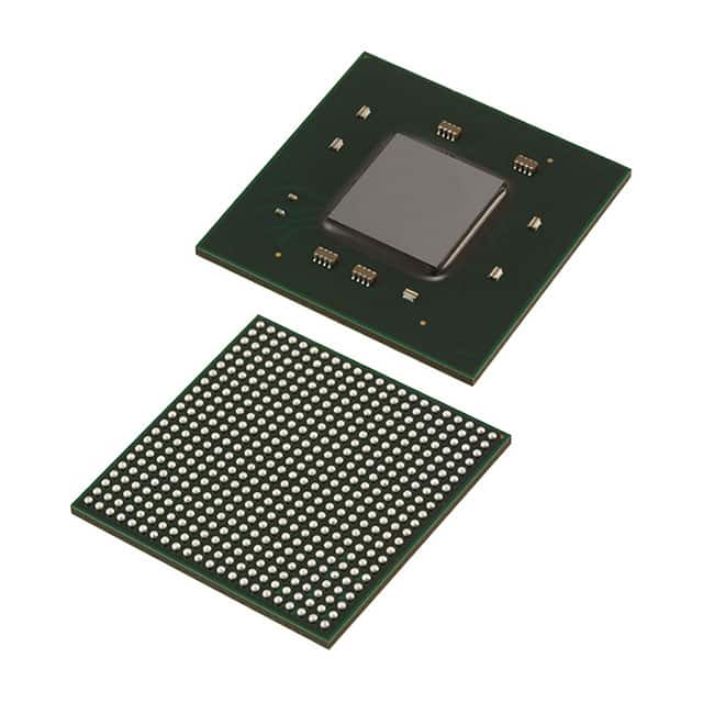
The XC7K70T-2FB484C comes in a FB484 package, which refers to a fine-pitch ball grid array (BGA) package with 484 solder balls.
Essence
The essence of the XC7K70T-2FB484C lies in its ability to provide a versatile platform for implementing complex digital designs. It allows users to create custom logic circuits tailored to their specific application requirements.
Packaging/Quantity
The XC7K70T-2FB484C is typically sold individually or in small quantities, depending on the supplier's packaging options.
Specifications
- Logic Cells: 68,200
- Flip-Flops: 136,400
- Block RAM: 4,860 Kb
- DSP Slices: 240
- Maximum I/O Pins: 400
- Operating Voltage: 1.0V - 1.2V
- Operating Temperature: -40°C to 100°C
Detailed Pin Configuration
The XC7K70T-2FB484C has a total of 400 I/O pins, each serving a specific purpose in the circuit design. For detailed pin configuration information, please refer to the manufacturer's datasheet.
Functional Features
- High-speed performance: The XC7K70T-2FB484C is designed to operate at high clock frequencies, enabling rapid data processing and real-time applications.
- Configurable I/Os: The FPGA offers a wide range of configurable I/O standards, allowing seamless integration with various external devices and interfaces.
- Embedded memory: With ample block RAM capacity, the XC7K70T-2FB484C can efficiently store and process large amounts of data.
- DSP capabilities: The integrated digital signal processing (DSP) slices enable efficient implementation of complex algorithms and signal processing tasks.
Advantages and Disadvantages
Advantages
- Flexibility: FPGAs like the XC7K70T-2FB484C provide the flexibility to modify and reconfigure the hardware design as needed, making them suitable for prototyping and iterative development.
- High-performance computing: The XC7K70T-2FB484C offers powerful computational capabilities, making it ideal for applications that require intensive data processing.
- Customizability: Users can tailor the FPGA's logic circuits to meet specific application requirements, resulting in optimized performance.
Disadvantages
- Complexity: Designing and programming an FPGA requires specialized knowledge and expertise, which may pose a challenge for beginners or those unfamiliar with digital circuit design.
- Power consumption: FPGAs tend to consume more power compared to other integrated circuits, especially when operating at high clock frequencies.
Working Principles
The XC7K70T-2FB484C operates based on the principles of reconfigurable computing. It consists of an array of programmable logic cells interconnected through configurable routing resources. These logic cells can be programmed to implement desired digital functions by configuring their interconnections and behavior.
The FPGA's configuration is stored in non-volatile memory, allowing it to retain the programmed design even after power is removed. During operation, the FPGA executes the programmed logic circuits, processing input data and generating output signals based on the defined functionality.
Detailed Application Field Plans
The XC7K70T-2FB484C finds applications in various fields, including:
- Communications: Used in wireless base stations, network routers, and communication infrastructure equipment for high-speed data processing and protocol handling.
- Aerospace and Defense: Employed in radar systems, avionics, and military-grade communication devices for their ability to handle complex algorithms and real-time signal processing.
- Industrial Automation: Utilized in industrial control systems, robotics, and machine vision applications to implement custom control algorithms and interface with sensors and actuators.
- Medical Devices: Integrated into medical imaging equipment, patient monitoring systems, and diagnostic devices to enable real-time image processing and data analysis.
- Research and Development: Used by researchers and developers for prototyping and testing new digital designs and algorithms before manufacturing custom ASICs.
Detailed and Complete Alternative Models
- XC7A100T-2FGG484C: A similar FPGA from the same family, offering a higher logic capacity and additional features. 2
רשום 10 שאלות ותשובות נפוצות הקשורות ליישום של XC7K70T-2FB484C בפתרונות טכניים
Sure! Here are 10 common questions and answers related to the application of XC7K70T-2FB484C in technical solutions:
Q: What is XC7K70T-2FB484C? A: XC7K70T-2FB484C is a specific model of Xilinx's Kintex-7 FPGA series, which is a programmable logic device used in various technical applications.
Q: What are the key features of XC7K70T-2FB484C? A: Some key features of XC7K70T-2FB484C include a high-performance FPGA fabric, integrated memory blocks, DSP slices, and multiple I/O interfaces.
Q: What are the typical applications of XC7K70T-2FB484C? A: XC7K70T-2FB484C is commonly used in applications such as wireless communication systems, video processing, industrial automation, aerospace, and defense.
Q: How can XC7K70T-2FB484C be programmed? A: XC7K70T-2FB484C can be programmed using Xilinx's Vivado Design Suite, which provides a comprehensive development environment for FPGA designs.
Q: What is the power consumption of XC7K70T-2FB484C? A: The power consumption of XC7K70T-2FB484C depends on the specific design and operating conditions. It is recommended to refer to the datasheet for detailed power specifications.
Q: Can XC7K70T-2FB484C be used in safety-critical applications? A: Yes, XC7K70T-2FB484C can be used in safety-critical applications. However, it is important to follow appropriate design practices and consider any necessary safety certifications.
Q: What is the maximum operating frequency of XC7K70T-2FB484C? A: The maximum operating frequency of XC7K70T-2FB484C depends on the specific design and implementation. It is recommended to refer to the datasheet for timing specifications.
Q: Can XC7K70T-2FB484C interface with external devices? A: Yes, XC7K70T-2FB484C supports various I/O standards and can interface with external devices such as sensors, memory modules, communication interfaces, and more.
Q: Are there any development boards available for XC7K70T-2FB484C? A: Yes, Xilinx offers development boards specifically designed for XC7K70T-2FB484C, which provide a platform for prototyping and testing FPGA-based designs.
Q: Where can I find technical documentation and support for XC7K70T-2FB484C? A: You can find technical documentation, datasheets, application notes, and support resources for XC7K70T-2FB484C on Xilinx's official website or by contacting their customer support.