

XC6VLX365T-2FFG1759I
Product Overview
Category
The XC6VLX365T-2FFG1759I belongs to the category of Field-Programmable Gate Arrays (FPGAs).
Use
FPGAs are integrated circuits that can be programmed after manufacturing. They are widely used in various electronic applications, including telecommunications, automotive, aerospace, and consumer electronics.
Characteristics
The XC6VLX365T-2FFG1759I is known for its high performance and versatility. It offers a large number of logic cells, memory blocks, and input/output pins, making it suitable for complex digital designs. It also provides advanced features such as embedded processors and high-speed serial interfaces.
Package
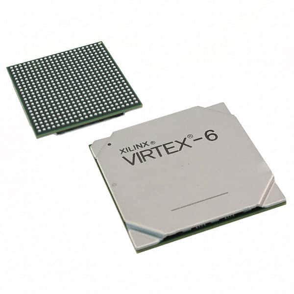
The XC6VLX365T-2FFG1759I comes in a Flip-Chip Fine-Pitch Ball Grid Array (FFG) package.
Essence
The essence of the XC6VLX365T-2FFG1759I lies in its ability to provide reconfigurable hardware, allowing designers to implement custom logic functions without the need for dedicated application-specific integrated circuits (ASICs).
Packaging/Quantity
The XC6VLX365T-2FFG1759I is typically sold individually or in small quantities, depending on the supplier.
Specifications
- Logic Cells: 362,880
- Memory Blocks: 4,608
- Input/Output Pins: 1,759
- Maximum Operating Frequency: 550 MHz
- Programmable Logic Slices: 5,760
- Embedded Multipliers: 768
- On-Chip RAM: 36 Mb
- Operating Voltage: 1.0V - 1.2V
Detailed Pin Configuration
The XC6VLX365T-2FFG1759I has a complex pin configuration, with multiple banks of input/output pins. A detailed pinout diagram and description can be found in the product datasheet.
Functional Features
- High-performance programmable logic cells for complex digital designs.
- Embedded processors for implementing soft-core microcontrollers.
- High-speed serial interfaces for communication with external devices.
- On-chip memory blocks for efficient data storage and retrieval.
- Flexible clock management resources for precise timing control.
Advantages and Disadvantages
Advantages
- Versatile and reconfigurable hardware platform.
- High-performance capabilities for demanding applications.
- Support for advanced features such as embedded processors and high-speed serial interfaces.
- Eliminates the need for custom ASIC development, reducing time-to-market.
Disadvantages
- Complexity may require specialized knowledge for effective utilization.
- Higher cost compared to traditional fixed-function integrated circuits.
- Power consumption can be relatively high, especially when operating at maximum performance.
Working Principles
The XC6VLX365T-2FFG1759I operates based on the principles of configurable logic. It consists of a matrix of programmable logic cells interconnected through configurable routing resources. The desired functionality is achieved by programming the interconnections and configuring the logic cells using Hardware Description Languages (HDLs) or graphical design tools.
Detailed Application Field Plans
The XC6VLX365T-2FFG1759I finds applications in various fields, including:
- Telecommunications: Used in base stations, routers, and network switches for high-speed data processing and protocol handling.
- Automotive: Employed in advanced driver assistance systems (ADAS), infotainment systems, and engine control units (ECUs) for enhanced performance and functionality.
- Aerospace: Utilized in satellite communication systems, avionics, and radar systems for their high reliability and flexibility.
- Consumer Electronics: Integrated into gaming consoles, high-definition televisions, and multimedia devices to enable complex signal processing and multimedia capabilities.
Detailed and Complete Alternative Models
- XC7A200T-2FBG676I: A newer FPGA model with enhanced performance and additional features.
- XC6SLX150T-3FGG484C: A lower-cost alternative with reduced logic capacity but suitable for less demanding applications.
- XC7Z020-1CLG400C: A hybrid FPGA and ARM processor model, combining the benefits of programmable logic and embedded processing.
These alternative models offer different trade-offs in terms of cost, performance, and features, allowing designers to choose the most suitable option for their specific requirements.
In conclusion, the XC6VLX365T-2FFG1759I is a high-performance FPGA that provides flexibility, advanced features, and reconfigurable hardware. It finds applications in various industries and offers advantages such as versatility and elimination of custom ASIC development. However, it also has some disadvantages, including complexity and higher cost. Designers can consider alternative models based on their specific needs.
רשום 10 שאלות ותשובות נפוצות הקשורות ליישום של XC6VLX365T-2FFG1759I בפתרונות טכניים
Sure! Here are 10 common questions and answers related to the application of XC6VLX365T-2FFG1759I in technical solutions:
Question: What is the XC6VLX365T-2FFG1759I?
- Answer: The XC6VLX365T-2FFG1759I is a high-performance field-programmable gate array (FPGA) manufactured by Xilinx.Question: What are the key features of the XC6VLX365T-2FFG1759I?
- Answer: The key features include a large number of logic cells, high-speed serial transceivers, embedded memory blocks, and various I/O options.Question: In what applications can the XC6VLX365T-2FFG1759I be used?
- Answer: It can be used in a wide range of applications such as telecommunications, networking, industrial automation, aerospace, and defense.Question: What is the maximum operating frequency of the XC6VLX365T-2FFG1759I?
- Answer: The maximum operating frequency depends on the specific design and implementation, but it can reach up to several hundred megahertz or even gigahertz.Question: How much logic capacity does the XC6VLX365T-2FFG1759I offer?
- Answer: It offers a logic capacity of approximately 365,000 logic cells, which can be used to implement complex digital designs.Question: Can the XC6VLX365T-2FFG1759I support high-speed serial communication?
- Answer: Yes, it has built-in high-speed serial transceivers that support protocols like PCIe, Ethernet, SATA, and USB.Question: What are the power requirements for the XC6VLX365T-2FFG1759I?
- Answer: The power requirements vary depending on the specific configuration and usage, but it typically operates at a voltage of 1.0V or 1.2V.Question: Does the XC6VLX365T-2FFG1759I have any built-in memory?
- Answer: Yes, it has embedded memory blocks that can be used for storing data or implementing memory-intensive functions.Question: Can the XC6VLX365T-2FFG1759I interface with other components or devices?
- Answer: Yes, it supports various I/O standards and can interface with external components such as sensors, displays, and communication modules.Question: What development tools are available for programming the XC6VLX365T-2FFG1759I?
- Answer: Xilinx provides a suite of development tools, including Vivado Design Suite, which allows designers to program and configure the FPGA efficiently.
Please note that the answers provided here are general and may vary based on specific design requirements and implementation details.