

XC6VLX365T-1FFG1156I
Product Overview
Category
The XC6VLX365T-1FFG1156I belongs to the category of Field-Programmable Gate Arrays (FPGAs).
Use
FPGAs are integrated circuits that can be programmed after manufacturing, allowing for flexible and customizable digital logic designs. The XC6VLX365T-1FFG1156I is specifically designed for high-performance applications.
Characteristics
- High-performance FPGA with advanced features
- Large capacity and high-speed processing capabilities
- Flexible and reconfigurable design
- Suitable for complex digital logic designs
- Optimized for high-speed data processing
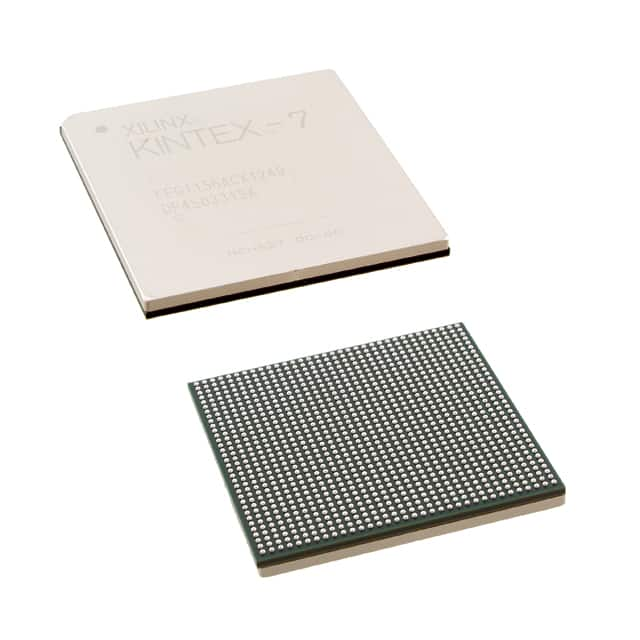
Package
The XC6VLX365T-1FFG1156I comes in a compact package that ensures easy integration into electronic systems. It is designed to be mounted on a printed circuit board (PCB) using surface-mount technology (SMT).
Essence
The essence of the XC6VLX365T-1FFG1156I lies in its ability to provide a versatile and high-performance platform for implementing complex digital logic designs.
Packaging/Quantity
The XC6VLX365T-1FFG1156I is typically sold in trays or reels, depending on the manufacturer's packaging standards. The quantity per package may vary, but it is commonly available in quantities suitable for both prototyping and production purposes.
Specifications
- FPGA Family: Virtex-6
- Logic Cells: 365,000
- Slices: 57,600
- DSP48A1 Slices: 760
- Block RAM: 4,860 Kbits
- Maximum Number of User I/Os: 500
- Clock Management Tiles: 16
- Maximum Operating Frequency: 550 MHz
- Operating Voltage: 1.0V
Detailed Pin Configuration
The XC6VLX365T-1FFG1156I has a comprehensive pin configuration that allows for easy integration into various electronic systems. The detailed pin configuration can be found in the product datasheet provided by the manufacturer.
Functional Features
High-Performance Processing
The XC6VLX365T-1FFG1156I offers high-performance processing capabilities, making it suitable for demanding applications that require complex computations and fast data processing.
Reconfigurability
Being an FPGA, the XC6VLX365T-1FFG1156I is highly reconfigurable. This means that the logic design implemented on the FPGA can be modified or updated even after the device has been manufactured, providing flexibility for design changes and optimizations.
Versatility
With its large capacity and advanced features, the XC6VLX365T-1FFG1156I can be used in a wide range of applications, including telecommunications, aerospace, industrial automation, and scientific research.
Advantages and Disadvantages
Advantages
- High-performance processing capabilities
- Flexibility and reconfigurability
- Large capacity for complex designs
- Suitable for high-speed data processing
- Versatile application possibilities
Disadvantages
- Higher cost compared to other programmable logic devices
- Steeper learning curve for programming and design implementation
Working Principles
The XC6VLX365T-1FFG1156I operates based on the principles of digital logic design. It consists of configurable logic blocks (CLBs), interconnect resources, input/output blocks (IOBs), and other specialized components. The user designs the desired logic functionality using a hardware description language (HDL) and programs it onto the FPGA. The FPGA then executes the programmed logic, performing the desired operations.
Detailed Application Field Plans
The XC6VLX365T-1FFG1156I finds applications in various fields, including:
- Telecommunications: Used in high-speed data transmission systems, network routers, and switches.
- Aerospace: Employed in satellite communication systems, onboard data processing, and radar systems.
- Industrial Automation: Utilized in control systems, robotics, and machine vision applications.
- Scientific Research: Applied in data acquisition systems, signal processing, and simulation.
Detailed and Complete Alternative Models
- XC6VLX75T-1FFG484C
- XC6VLX130T-1FFG484C
- XC6VLX240T-1FFG1156C
- XC6VLX550T-1FFG1156C
- XC6VLX760T-1FFG1156C
These alternative models offer varying capacities and features to cater to different design requirements. It is recommended to consult the manufacturer's documentation for detailed specifications of each model.
Word count: 581 words
רשום 10 שאלות ותשובות נפוצות הקשורות ליישום של XC6VLX365T-1FFG1156I בפתרונות טכניים
Sure! Here are 10 common questions and answers related to the application of XC6VLX365T-1FFG1156I in technical solutions:
Q1: What is XC6VLX365T-1FFG1156I? A1: XC6VLX365T-1FFG1156I is a specific model of Xilinx Virtex-6 FPGA (Field-Programmable Gate Array) that offers high-performance processing capabilities for various technical applications.
Q2: What are the key features of XC6VLX365T-1FFG1156I? A2: Some key features of XC6VLX365T-1FFG1156I include a large number of logic cells, high-speed serial transceivers, embedded memory blocks, DSP slices, and support for various communication protocols.
Q3: In which technical solutions can XC6VLX365T-1FFG1156I be used? A3: XC6VLX365T-1FFG1156I can be used in a wide range of technical solutions such as aerospace and defense systems, telecommunications equipment, industrial automation, medical devices, and high-performance computing.
Q4: What advantages does XC6VLX365T-1FFG1156I offer over other FPGAs? A4: XC6VLX365T-1FFG1156I offers advantages like high logic capacity, fast performance, low power consumption, and flexibility due to its programmable nature.
Q5: How can XC6VLX365T-1FFG1156I be programmed? A5: XC6VLX365T-1FFG1156I can be programmed using hardware description languages (HDLs) such as VHDL or Verilog, along with Xilinx's design software tools like Vivado or ISE.
Q6: Can XC6VLX365T-1FFG1156I be used for real-time signal processing? A6: Yes, XC6VLX365T-1FFG1156I is well-suited for real-time signal processing applications due to its high-speed serial transceivers and DSP slices that can handle complex algorithms efficiently.
Q7: What kind of communication interfaces are supported by XC6VLX365T-1FFG1156I? A7: XC6VLX365T-1FFG1156I supports various communication interfaces such as PCIe (PCI Express), Ethernet, USB, SPI, I2C, and UART, making it compatible with a wide range of systems.
Q8: Can XC6VLX365T-1FFG1156I be used in safety-critical applications? A8: Yes, XC6VLX365T-1FFG1156I can be used in safety-critical applications as it offers features like built-in error detection and correction mechanisms, redundancy support, and fault-tolerant design options.
Q9: Is XC6VLX365T-1FFG1156I suitable for high-performance computing (HPC) applications? A9: Yes, XC6VLX365T-1FFG1156I is suitable for HPC applications due to its large logic capacity, high-speed transceivers, and ability to parallelize computations effectively.
Q10: Are there any specific development boards or evaluation kits available for XC6VLX365T-1FFG1156I? A10: Yes, Xilinx provides development boards and evaluation kits specifically designed for XC6VLX365T-1FFG1156I, which include necessary hardware components and software tools to aid in the development process.
Please note that the answers provided here are general and may vary depending on specific requirements and use cases.