

XC4003E-1PC84C
Product Overview
Category
XC4003E-1PC84C belongs to the category of programmable logic devices (PLDs).
Use
This product is commonly used in digital circuit design and implementation. It provides a flexible and customizable solution for various applications.
Characteristics
- Programmable: The XC4003E-1PC84C can be programmed to perform specific functions according to the user's requirements.
- High Integration: It integrates multiple logic gates, flip-flops, and other components into a single device, reducing the need for external components.
- Versatile: It can be used in a wide range of applications, including telecommunications, industrial control systems, consumer electronics, and more.
Package
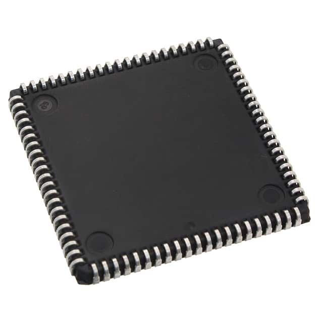
The XC4003E-1PC84C is available in a 84-pin plastic leaded chip carrier (PLCC) package.
Essence
The essence of XC4003E-1PC84C lies in its ability to provide reconfigurable logic functions, allowing designers to implement complex digital circuits efficiently.
Packaging/Quantity
The XC4003E-1PC84C is typically packaged in tubes or trays, with a quantity of 25 units per tube/tray.
Specifications
- Logic Cells: 4000
- Maximum Operating Frequency: 50 MHz
- Number of I/O Pins: 68
- Supply Voltage: 5V
- Operating Temperature Range: -40°C to +85°C
Detailed Pin Configuration
The XC4003E-1PC84C has a total of 84 pins. Here is a brief overview of some key pin functions:
- VCC: Power supply voltage input
- GND: Ground reference
- CLK: Clock input for synchronous operations
- I/O Pins: General-purpose input/output pins
- JTAG Pins: Pins for Joint Test Action Group (JTAG) boundary scan testing
For a complete pin configuration diagram, please refer to the product datasheet.
Functional Features
- Reconfigurable Logic: The XC4003E-1PC84C can be programmed to implement various logic functions, allowing for flexibility in circuit design.
- Fast Operation: With a maximum operating frequency of 50 MHz, it can handle high-speed digital signals effectively.
- I/O Flexibility: The device offers a sufficient number of I/O pins for interfacing with external components and devices.
- JTAG Support: The JTAG pins enable boundary scan testing, facilitating debugging and verification processes.
Advantages and Disadvantages
Advantages
- Flexibility: The reconfigurable nature of the XC4003E-1PC84C allows for easy modifications and updates to the circuit design.
- Integration: It integrates multiple logic components into a single device, reducing the need for additional external components.
- Versatility: The XC4003E-1PC84C can be used in various applications due to its wide range of programmable functions.
Disadvantages
- Limited Resources: The XC4003E-1PC84C has a finite number of logic cells and I/O pins, which may restrict the complexity of designs.
- Power Consumption: As with most programmable logic devices, power consumption can be relatively high compared to dedicated hardware solutions.
Working Principles
The XC4003E-1PC84C utilizes a combination of programmable logic blocks, interconnect resources, and input/output elements to implement user-defined logic functions. These functions are configured by programming the device using specialized software tools. During operation, the programmed configuration is stored in non-volatile memory within the device, allowing it to retain the desired functionality even after power is removed.
Detailed Application Field Plans
The XC4003E-1PC84C can be applied in various fields, including:
- Telecommunications: It can be used in the design of communication systems, such as data routers and network switches.
- Industrial Control Systems: The XC4003E-1PC84C is suitable for implementing control logic in industrial automation systems.
- Consumer Electronics: It finds applications in devices like gaming consoles, digital cameras, and audio/video equipment.
- Automotive Electronics: It can be utilized in automotive control units, providing customizable functionality for vehicle systems.
Detailed and Complete Alternative Models
- XC4003E-1PQ100C: Similar to XC4003E-1PC84C but available in a 100-pin plastic quad flat pack (PQFP) package.
- XC4003E-2PC84C: A higher-density version with double the number of logic cells, available in the same 84-pin PLCC package.
- XC4003E-3PQ160C: A larger variant with increased logic capacity, packaged in a 160-pin PQFP package.
These alternative models offer different pin configurations, logic capacities, and package
רשום 10 שאלות ותשובות נפוצות הקשורות ליישום של XC4003E-1PC84C בפתרונות טכניים
Sure! Here are 10 common questions and answers related to the application of XC4003E-1PC84C in technical solutions:
Q1: What is XC4003E-1PC84C? A1: XC4003E-1PC84C is a specific model of Field Programmable Gate Array (FPGA) manufactured by Xilinx.
Q2: What are the key features of XC4003E-1PC84C? A2: Some key features of XC4003E-1PC84C include 4000 gates, 84-pin plastic package, and low power consumption.
Q3: What are the typical applications of XC4003E-1PC84C? A3: XC4003E-1PC84C is commonly used in various applications such as digital signal processing, telecommunications, industrial control systems, and embedded systems.
Q4: How can I program XC4003E-1PC84C? A4: XC4003E-1PC84C can be programmed using Xilinx's proprietary software tools like Vivado or ISE Design Suite.
Q5: Can XC4003E-1PC84C be used for high-speed data processing? A5: Yes, XC4003E-1PC84C is capable of handling high-speed data processing due to its efficient architecture and advanced features.
Q6: What is the maximum operating frequency of XC4003E-1PC84C? A6: The maximum operating frequency of XC4003E-1PC84C depends on the specific design and implementation, but it can typically reach frequencies in the range of tens to hundreds of megahertz.
Q7: Can XC4003E-1PC84C interface with other components or devices? A7: Yes, XC4003E-1PC84C can interface with various components and devices through its I/O pins, allowing for seamless integration into larger systems.
Q8: Is XC4003E-1PC84C suitable for low-power applications? A8: Yes, XC4003E-1PC84C is designed to be power-efficient, making it suitable for low-power applications where minimizing energy consumption is important.
Q9: Can XC4003E-1PC84C be reprogrammed after deployment? A9: Yes, XC4003E-1PC84C is a field-programmable device, which means it can be reprogrammed even after it has been deployed in a system.
Q10: Are there any limitations or considerations when using XC4003E-1PC84C? A10: Some considerations include the limited number of gates compared to more modern FPGAs, potential compatibility issues with newer software tools, and the need for expertise in FPGA design to fully utilize its capabilities.