

XC3S50-5VQG100C
Product Overview
Category
The XC3S50-5VQG100C belongs to the category of Field-Programmable Gate Arrays (FPGAs).
Use
FPGAs are integrated circuits that can be programmed and reprogrammed to perform various digital functions. The XC3S50-5VQG100C is specifically designed for applications requiring moderate logic capacity and high-performance features.
Characteristics
- Moderate logic capacity
- High-performance features
- Programmable and reprogrammable
- Versatile functionality
Package
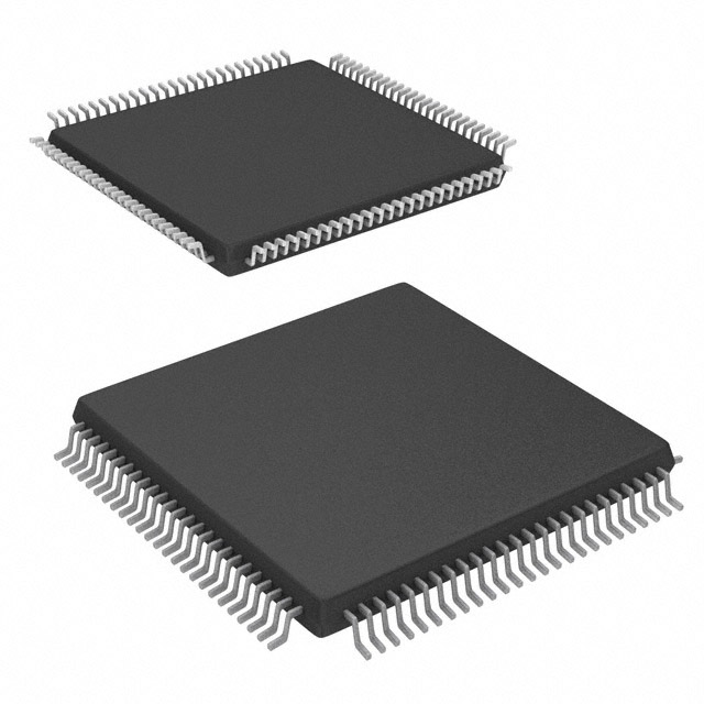
The XC3S50-5VQG100C comes in a Quad Flat No-Lead (QFN) package.
Essence
The essence of the XC3S50-5VQG100C lies in its ability to provide flexible and customizable digital logic functions, making it suitable for a wide range of applications.
Packaging/Quantity
The XC3S50-5VQG100C is typically packaged in reels or trays, with a quantity of 100 units per package.
Specifications
- Logic Cells: 3,456
- Flip-Flops: 2,304
- Block RAM: 54 Kb
- Maximum Frequency: 250 MHz
- I/O Pins: 100
- Operating Voltage: 5V
- Package Type: QFN
- Temperature Range: -40°C to +85°C
Detailed Pin Configuration
The XC3S50-5VQG100C has a total of 100 I/O pins. These pins are used for input and output connections to external devices. The pin configuration is as follows:
(Pin Number) - (Pin Name) 1 - VCCIO 2 - GND 3 - IO0 4 - IO1 5 - IO2 ... 100 - IO99
Functional Features
The XC3S50-5VQG100C offers several functional features that enhance its performance and usability. These include:
- Programmability: The FPGA can be programmed to implement various digital functions, allowing for flexibility and customization.
- High-Speed Operation: With a maximum frequency of 250 MHz, the XC3S50-5VQG100C can handle high-speed data processing.
- Versatility: The FPGA supports a wide range of applications due to its moderate logic capacity and high-performance features.
Advantages and Disadvantages
Advantages
- Flexibility and reprogrammability
- High-performance capabilities
- Versatile functionality
- Moderate logic capacity suitable for various applications
Disadvantages
- Limited logic capacity compared to larger FPGAs
- Higher power consumption compared to low-power alternatives
Working Principles
The XC3S50-5VQG100C operates based on the principles of configurable logic blocks (CLBs) and interconnect resources. CLBs consist of look-up tables (LUTs), flip-flops, and multiplexers, which can be configured to perform specific logic functions. Interconnect resources provide routing paths between CLBs, enabling the flow of data within the FPGA.
Detailed Application Field Plans
The XC3S50-5VQG100C finds applications in various fields, including:
- Communications: Used in networking equipment, routers, and switches for data processing and protocol handling.
- Industrial Automation: Employed in control systems, robotics, and machine vision applications for real-time data processing and control.
- Automotive: Utilized in automotive electronics for functions such as engine control, driver assistance systems, and infotainment.
- Aerospace: Applied in avionics systems for flight control, navigation, and communication purposes.
Detailed and Complete Alternative Models
- XC3S200-4VQG100C: Offers higher logic capacity and more I/O pins compared to the XC3S50-5VQG100C.
- XC3S1000-5VQG100C: Provides significantly larger logic capacity and additional features for more complex applications.
- XC3S4000-6VQG100C: Designed for high-performance applications requiring extensive logic capacity and advanced functionality.
These alternative models offer varying levels of logic capacity, I/O pins, and performance features to cater to different application requirements.
Word count: 550 words
רשום 10 שאלות ותשובות נפוצות הקשורות ליישום של XC3S50-5VQG100C בפתרונות טכניים
Sure! Here are 10 common questions and answers related to the application of XC3S50-5VQG100C in technical solutions:
Question: What is XC3S50-5VQG100C?
Answer: XC3S50-5VQG100C is a specific model of Field-Programmable Gate Array (FPGA) manufactured by Xilinx.Question: What is an FPGA?
Answer: FPGA stands for Field-Programmable Gate Array, which is a type of integrated circuit that can be programmed or reconfigured after manufacturing.Question: What are the key features of XC3S50-5VQG100C?
Answer: Some key features of XC3S50-5VQG100C include 50,000 system gates, 36Kbits of block RAM, 4 Digital Clock Managers (DCMs), and support for various I/O standards.Question: In what applications can XC3S50-5VQG100C be used?
Answer: XC3S50-5VQG100C can be used in a wide range of applications such as digital signal processing, embedded systems, communication systems, industrial automation, and more.Question: How can XC3S50-5VQG100C be programmed?
Answer: XC3S50-5VQG100C can be programmed using Xilinx's Vivado Design Suite or other compatible programming tools.Question: What is the power supply requirement for XC3S50-5VQG100C?
Answer: XC3S50-5VQG100C requires a 5V power supply for proper operation.Question: Can XC3S50-5VQG100C interface with other devices?
Answer: Yes, XC3S50-5VQG100C supports various communication interfaces such as SPI, I2C, UART, and GPIOs, allowing it to interface with other devices.Question: What is the maximum operating frequency of XC3S50-5VQG100C?
Answer: The maximum operating frequency of XC3S50-5VQG100C depends on the specific design and implementation, but it can typically reach frequencies in the range of tens to hundreds of megahertz.Question: Can XC3S50-5VQG100C be used for prototyping or production?
Answer: XC3S50-5VQG100C can be used for both prototyping and small-scale production. For larger production volumes, a different FPGA model may be more suitable.Question: Are there any development boards available for XC3S50-5VQG100C?
Answer: Yes, Xilinx offers development boards like the Spartan-3E Starter Kit that are compatible with XC3S50-5VQG100C and provide a convenient platform for evaluation and development.
Please note that these answers are general and may vary depending on the specific requirements and use cases.