

XC3S50-4VQG100I
Product Overview
Category
The XC3S50-4VQG100I belongs to the category of Field-Programmable Gate Arrays (FPGAs).
Use
FPGAs are integrated circuits that can be programmed and reprogrammed to perform various digital functions. The XC3S50-4VQG100I is specifically designed for applications requiring moderate logic capacity and high-performance features.
Characteristics
- Moderate logic capacity
- High-performance features
- Programmable and reprogrammable
- Versatile functionality
Package
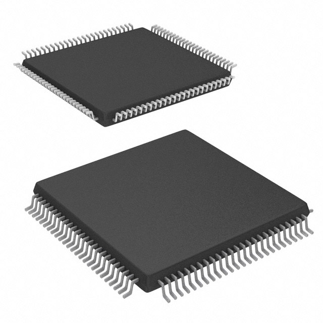
The XC3S50-4VQG100I comes in a Quad Flat No-Lead (QFN) package.
Essence
The essence of the XC3S50-4VQG100I lies in its ability to provide flexible and customizable digital circuitry, allowing designers to implement complex logic functions in a single chip.
Packaging/Quantity
The XC3S50-4VQG100I is typically packaged in reels or trays, with each reel or tray containing a specific quantity of chips. The exact packaging and quantity may vary depending on the supplier.
Specifications
- Logic Cells: 5,000
- Flip-Flops: 2,500
- Look-Up Tables (LUTs): 2,500
- Maximum Frequency: 250 MHz
- I/O Pins: 100
- Operating Voltage: 1.2V
- Operating Temperature Range: -40°C to 100°C
Detailed Pin Configuration
The XC3S50-4VQG100I has a total of 100 I/O pins, which are used for input and output connections. These pins are arranged in a specific configuration to facilitate easy integration into electronic systems. A detailed pin configuration diagram can be found in the product datasheet.
Functional Features
- High logic capacity for implementing complex digital functions
- Fast operating frequency for high-performance applications
- Flexible I/O configuration for interfacing with external devices
- On-chip memory blocks for data storage and processing
- Built-in clock management resources for precise timing control
Advantages and Disadvantages
Advantages
- Versatile and customizable functionality
- Reconfigurable nature allows for easy updates and modifications
- Reduced development time compared to custom ASIC designs
- Lower cost compared to dedicated hardware solutions for specific applications
Disadvantages
- Higher power consumption compared to application-specific integrated circuits (ASICs)
- Limited logic capacity compared to larger FPGAs
- Longer design iteration cycles due to the need for programming and verification
Working Principles
The XC3S50-4VQG100I operates based on the principles of configurable logic. It consists of an array of programmable logic cells, interconnected by a network of configurable routing resources. The logic cells can be programmed to implement various digital functions, while the routing resources allow for the interconnection of these cells to create complex circuits.
Detailed Application Field Plans
The XC3S50-4VQG100I finds applications in various fields, including:
- Communications: Used in wireless base stations, routers, and network switches for signal processing and protocol implementation.
- Industrial Automation: Employed in control systems, motor drives, and robotics for real-time control and monitoring.
- Automotive: Integrated into automotive electronics for functions like engine control, driver assistance systems, and infotainment.
- Aerospace and Defense: Utilized in radar systems, avionics, and military communication equipment for high-performance signal processing and encryption.
Detailed and Complete Alternative Models
- XC3S200-4VQG100I: Offers higher logic capacity and more I/O pins for larger-scale applications.
- XC3S1000-4VQG100I: Provides significantly higher logic capacity and advanced features for complex designs.
- XC3S4000-4VQG100I: Designed for applications requiring extensive logic resources and high-performance requirements.
These alternative models offer varying levels of logic capacity, I/O pins, and performance to cater to different application needs.
Word count: 540 words
רשום 10 שאלות ותשובות נפוצות הקשורות ליישום של XC3S50-4VQG100I בפתרונות טכניים
Sure! Here are 10 common questions and answers related to the application of XC3S50-4VQG100I in technical solutions:
Question: What is XC3S50-4VQG100I?
Answer: XC3S50-4VQG100I is a specific model of Field-Programmable Gate Array (FPGA) manufactured by Xilinx.Question: What is an FPGA?
Answer: FPGA stands for Field-Programmable Gate Array, which is a type of integrated circuit that can be programmed or reconfigured after manufacturing.Question: What are the key features of XC3S50-4VQG100I?
Answer: Some key features of XC3S50-4VQG100I include 50,000 system gates, 36Kbits of block RAM, 64 user I/O pins, and a maximum operating frequency of 400MHz.Question: In what applications can XC3S50-4VQG100I be used?
Answer: XC3S50-4VQG100I can be used in various applications such as digital signal processing, industrial automation, robotics, telecommunications, and embedded systems.Question: How can XC3S50-4VQG100I be programmed?
Answer: XC3S50-4VQG100I can be programmed using Hardware Description Languages (HDLs) like VHDL or Verilog, or through Xilinx's proprietary software tools like Vivado or ISE.Question: What is the power supply requirement for XC3S50-4VQG100I?
Answer: XC3S50-4VQG100I typically requires a power supply voltage of 1.14V to 1.26V.Question: Can XC3S50-4VQG100I interface with other components or devices?
Answer: Yes, XC3S50-4VQG100I can interface with other components or devices through its user I/O pins, which can be configured as inputs or outputs.Question: What is the maximum operating frequency of XC3S50-4VQG100I?
Answer: The maximum operating frequency of XC3S50-4VQG100I is 400MHz, meaning it can process signals up to that frequency.Question: Can XC3S50-4VQG100I be used for real-time applications?
Answer: Yes, XC3S50-4VQG100I can be used for real-time applications as it offers high-speed processing capabilities and low-latency communication.Question: Are there any development boards available for XC3S50-4VQG100I?
Answer: Yes, Xilinx provides development boards like the Spartan-3E Starter Kit that can be used for prototyping and testing XC3S50-4VQG100I-based designs.
Please note that the answers provided here are general and may vary depending on specific requirements and use cases.