

XC3S1600E-4FGG320C
Product Overview
Category
The XC3S1600E-4FGG320C belongs to the category of Field Programmable Gate Arrays (FPGAs).
Use
FPGAs are integrated circuits that can be programmed after manufacturing. They are widely used in various electronic applications, including telecommunications, automotive, aerospace, and consumer electronics.
Characteristics
- The XC3S1600E-4FGG320C is a high-performance FPGA with advanced features.
- It offers a large number of programmable logic cells, allowing for complex digital designs.
- The device supports various I/O standards, making it versatile for different interface requirements.
- It has a high-speed serial interface, enabling fast data transfer rates.
- The FPGA is designed to be power-efficient, reducing energy consumption.
Package
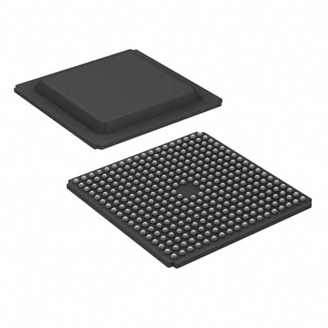
The XC3S1600E-4FGG320C comes in a compact package, which ensures easy integration into electronic systems. The package type is FG320, indicating a fine-pitch grid array with 320 pins.
Essence
The essence of the XC3S1600E-4FGG320C lies in its ability to provide flexible and customizable digital circuitry. Its programmable nature allows designers to implement specific functionalities according to their requirements.
Packaging/Quantity
The XC3S1600E-4FGG320C is typically packaged individually and is available in various quantities depending on the manufacturer or distributor.
Specifications
- Logic Cells: 1,600
- Maximum Frequency: 500 MHz
- Block RAM: 576 Kb
- DSP Slices: 48
- I/O Pins: 320
- Operating Voltage: 1.2V
- Package Type: FG320
Detailed Pin Configuration
The XC3S1600E-4FGG320C has a total of 320 pins, each serving a specific purpose in the FPGA's functionality. The pin configuration includes input/output pins, power supply pins, clock pins, and configuration pins. For a detailed pin configuration diagram, please refer to the manufacturer's datasheet.
Functional Features
- High-performance programmable logic cells for complex digital designs.
- Versatile I/O standards for interfacing with different devices.
- High-speed serial interface for fast data transfer.
- Power-efficient design for reduced energy consumption.
- Configurable memory blocks for efficient storage and retrieval of data.
- Built-in digital signal processing (DSP) slices for implementing advanced algorithms.
Advantages and Disadvantages
Advantages
- Flexibility: The XC3S1600E-4FGG320C allows designers to create custom digital circuits tailored to their specific needs.
- Time-to-Market: FPGAs enable rapid prototyping and development cycles, reducing time-to-market for electronic products.
- Reconfigurability: The ability to reprogram the FPGA allows for easy updates or modifications to the design without requiring hardware changes.
- Integration: FPGAs can integrate multiple functions into a single chip, reducing the need for additional components.
Disadvantages
- Complexity: Designing with FPGAs requires specialized knowledge and expertise.
- Cost: FPGAs can be more expensive compared to other integrated circuits due to their complexity and programmability.
- Power Consumption: While efforts have been made to improve power efficiency, FPGAs generally consume more power compared to application-specific integrated circuits (ASICs).
Working Principles
FPGAs consist of an array of configurable logic blocks interconnected through programmable interconnects. These logic blocks can be programmed to implement various digital functions using a hardware description language (HDL). The programming process involves specifying the desired logic connections and behavior, which is then compiled and loaded onto the FPGA.
Once programmed, the FPGA operates based on the specified logic connections, allowing it to perform complex digital operations. The reconfigurable nature of FPGAs enables them to be used in a wide range of applications, as their functionality can be easily modified or updated.
Detailed Application Field Plans
The XC3S1600E-4FGG320C finds application in various fields, including:
- Telecommunications: FPGAs are used in network infrastructure equipment, such as routers and switches, for high-speed data processing and protocol handling.
- Automotive: FPGAs play a crucial role in automotive electronics, enabling advanced driver assistance systems (ADAS), infotainment systems, and engine control units (ECUs).
- Aerospace: FPGAs are utilized in aerospace applications for tasks like satellite communication, radar signal processing, and flight control systems.
- Consumer Electronics: FPGAs are found in devices like smartphones, tablets, and gaming consoles, providing customizable features and improved performance.
Detailed and Complete Alternative Models
- XC7A35T-1CPG236C
- EP4CE6F17
רשום 10 שאלות ותשובות נפוצות הקשורות ליישום של XC3S1600E-4FGG320C בפתרונות טכניים
Sure! Here are 10 common questions and answers related to the application of XC3S1600E-4FGG320C in technical solutions:
Q: What is XC3S1600E-4FGG320C? A: XC3S1600E-4FGG320C is a field-programmable gate array (FPGA) manufactured by Xilinx. It offers 1,600K logic cells and operates at a speed grade of -4.
Q: What are some typical applications for XC3S1600E-4FGG320C? A: XC3S1600E-4FGG320C is commonly used in various technical solutions such as digital signal processing, high-speed data communication, industrial automation, and embedded systems.
Q: What is the maximum operating frequency of XC3S1600E-4FGG320C? A: The maximum operating frequency of XC3S1600E-4FGG320C depends on the design and implementation, but it can typically reach frequencies up to several hundred megahertz (MHz).
Q: How much programmable logic is available in XC3S1600E-4FGG320C? A: XC3S1600E-4FGG320C provides 1,600K logic cells, which can be used to implement complex digital designs.
Q: Can XC3S1600E-4FGG320C interface with external devices? A: Yes, XC3S1600E-4FGG320C supports various I/O standards and can interface with external devices such as memories, sensors, displays, and communication interfaces.
Q: What development tools are available for programming XC3S1600E-4FGG320C? A: Xilinx provides Vivado Design Suite, which includes tools for designing, simulating, synthesizing, and programming XC3S1600E-4FGG320C.
Q: Can XC3S1600E-4FGG320C be reprogrammed after deployment? A: Yes, XC3S1600E-4FGG320C is a reprogrammable FPGA, allowing for updates and modifications to the design even after it has been deployed in a technical solution.
Q: What are the power requirements for XC3S1600E-4FGG320C? A: The power requirements for XC3S1600E-4FGG320C depend on the specific design and configuration. It typically operates at a voltage of 1.2V or 3.3V.
Q: Is there any built-in security features in XC3S1600E-4FGG320C? A: XC3S1600E-4FGG320C offers various security features such as bitstream encryption, authentication, and tamper detection to protect the intellectual property and secure the design.
Q: Are there any limitations or considerations when using XC3S1600E-4FGG320C? A: Some considerations include power consumption, thermal management, I/O voltage compatibility, and the need for proper design and verification techniques to ensure reliable operation.
Please note that these answers are general and may vary depending on the specific implementation and requirements of your technical solution.