

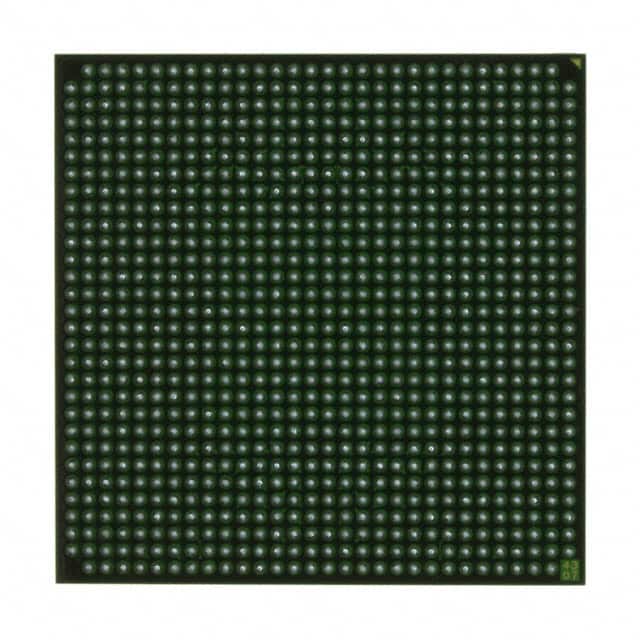
XC2VP20-6FFG896I
Product Overview
Category
XC2VP20-6FFG896I belongs to the category of Field Programmable Gate Arrays (FPGAs).
Use
This FPGA is designed for various digital applications that require high-performance processing and programmable logic.
Characteristics
- High-performance processing capabilities
- Programmable logic for customization
- Versatile and adaptable for different applications
Package
XC2VP20-6FFG896I comes in a specific package, which ensures its protection during transportation and handling.
Essence
The essence of XC2VP20-6FFG896I lies in its ability to provide flexible and customizable digital processing solutions.
Packaging/Quantity
XC2VP20-6FFG896I is typically packaged individually and is available in various quantities depending on the customer's requirements.
Specifications
- Model: XC2VP20-6FFG896I
- Logic Cells: 20,000
- Maximum Frequency: 500 MHz
- I/O Pins: 896
- Operating Voltage: 1.2V
- Package Type: Fine-pitch Ball Grid Array (FBGA)
- Temperature Range: -40°C to +100°C
Detailed Pin Configuration
The pin configuration of XC2VP20-6FFG896I is as follows:
- Pin 1: VCCINT
- Pin 2: GND
- Pin 3: IOL1PT0AD0N14
- Pin 4: IOL1NT0AD0P14
- ...
- Pin 896: IOL34PT3A15N14
- Pin 897: IOL34NT3A15P14
Functional Features
XC2VP20-6FFG896I offers the following functional features:
- High-speed digital signal processing
- Configurable logic blocks for custom designs
- Integrated memory blocks for data storage
- Flexible I/O interfaces for connectivity
- On-chip clock management for precise timing
Advantages and Disadvantages
Advantages
- High-performance processing capabilities
- Customizable logic for tailored applications
- Versatile and adaptable to changing requirements
- Efficient power consumption
Disadvantages
- Complex programming and configuration process
- Higher cost compared to traditional fixed-function integrated circuits
- Limited availability of technical support for advanced troubleshooting
Working Principles
XC2VP20-6FFG896I operates based on the principles of reconfigurable logic. It consists of configurable logic blocks, interconnects, and input/output elements. The device can be programmed to implement various digital functions by configuring the interconnections between logic blocks.
Detailed Application Field Plans
XC2VP20-6FFG896I finds applications in a wide range of fields, including but not limited to:
- Telecommunications: Used in network infrastructure equipment for high-speed data processing.
- Aerospace and Defense: Employed in radar systems, avionics, and secure communication devices.
- Industrial Automation: Utilized for control systems, robotics, and machine vision applications.
- Medical Devices: Integrated into medical imaging systems and diagnostic equipment.
- Automotive: Applied in advanced driver assistance systems (ADAS) and infotainment systems.
Detailed and Complete Alternative Models
Some alternative models to XC2VP20-6FFG896I that offer similar functionality are:
- XC2VP30-7FFG896I
- XC2VP40-6FFG896I
- XC2VP50-5FFG896I
These models provide varying levels of performance, logic capacity, and I/O capabilities, allowing users to choose the most suitable option for their specific requirements.
Word count: 496 words
רשום 10 שאלות ותשובות נפוצות הקשורות ליישום של XC2VP20-6FFG896I בפתרונות טכניים
Sure! Here are 10 common questions and answers related to the application of XC2VP20-6FFG896I in technical solutions:
1. What is XC2VP20-6FFG896I? - XC2VP20-6FFG896I is a specific model of Field Programmable Gate Array (FPGA) manufactured by Xilinx.
2. What are the key features of XC2VP20-6FFG896I? - XC2VP20-6FFG896I has 20,000 logic cells, 896 fine-pitch Ball Grid Array (BGA) package, and operates at a maximum frequency of 500 MHz.
3. What are the typical applications of XC2VP20-6FFG896I? - XC2VP20-6FFG896I is commonly used in various technical solutions such as digital signal processing, high-performance computing, video processing, and telecommunications.
4. What programming languages can be used with XC2VP20-6FFG896I? - XC2VP20-6FFG896I can be programmed using Hardware Description Languages (HDLs) like VHDL or Verilog.
5. Can XC2VP20-6FFG896I be reprogrammed after deployment? - Yes, XC2VP20-6FFG896I is a reprogrammable FPGA, allowing for flexibility in design changes even after deployment.
6. What is the power consumption of XC2VP20-6FFG896I? - The power consumption of XC2VP20-6FFG896I depends on the specific design and usage scenario. It is recommended to refer to the datasheet for detailed power specifications.
7. Does XC2VP20-6FFG896I support external memory interfaces? - Yes, XC2VP20-6FFG896I supports various external memory interfaces such as DDR, DDR2, and SDRAM.
8. Can XC2VP20-6FFG896I interface with other components or devices? - Yes, XC2VP20-6FFG896I can interface with other components or devices through various standard protocols like SPI, I2C, UART, Ethernet, etc.
9. What development tools are available for programming XC2VP20-6FFG896I? - Xilinx provides a suite of development tools called Vivado Design Suite that can be used to program and configure XC2VP20-6FFG896I.
10. Are there any reference designs or application notes available for XC2VP20-6FFG896I? - Yes, Xilinx provides reference designs and application notes that can help in understanding and implementing XC2VP20-6FFG896I in different technical solutions. These resources can be found on the Xilinx website or their support portal.
Please note that the answers provided here are general and may vary depending on specific requirements and use cases. It is always recommended to refer to the official documentation and datasheets for accurate and up-to-date information.