

XC2V1500-5BG575I
Product Overview
Category
The XC2V1500-5BG575I belongs to the category of Field Programmable Gate Arrays (FPGAs).
Use
FPGAs are integrated circuits that can be programmed and reprogrammed to perform various digital functions. The XC2V1500-5BG575I is specifically designed for high-performance applications that require complex logic functions.
Characteristics
- High-performance FPGA with advanced features
- Large capacity and high-speed processing capabilities
- Flexible and reconfigurable design
- Suitable for a wide range of applications
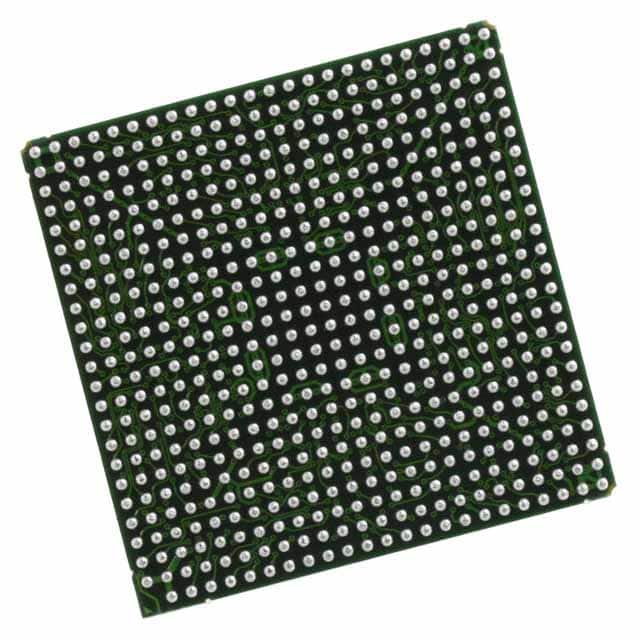
Package
The XC2V1500-5BG575I comes in a compact Ball Grid Array (BGA) package, which provides excellent thermal performance and allows for easy integration onto circuit boards.
Essence
The essence of the XC2V1500-5BG575I lies in its ability to provide customizable digital logic functions, enabling designers to implement complex algorithms and systems on a single chip.
Packaging/Quantity
The XC2V1500-5BG575I is typically packaged individually and is available in varying quantities depending on the manufacturer's specifications.
Specifications
- FPGA Family: Virtex-II
- Logic Cells: 1,500
- System Gates: 1,000,000
- Maximum Frequency: 400 MHz
- I/O Pins: 575
- Operating Voltage: 3.3V
- Package Type: BGA
- Temperature Range: -40°C to +85°C
Detailed Pin Configuration
The XC2V1500-5BG575I has 575 I/O pins, each serving a specific purpose in the overall functionality of the FPGA. A detailed pin configuration diagram can be found in the product datasheet provided by the manufacturer.
Functional Features
- High-speed data processing capabilities
- Configurable logic blocks for implementing complex algorithms
- On-chip memory resources for data storage
- Built-in digital signal processing (DSP) blocks for efficient signal processing
- Flexible I/O interfaces for seamless integration with external devices
Advantages and Disadvantages
Advantages
- High-performance FPGA suitable for demanding applications
- Reconfigurable design allows for flexibility in system development
- Large capacity enables implementation of complex logic functions
- Advanced features enhance overall system performance
Disadvantages
- Higher cost compared to other programmable logic devices
- Steeper learning curve for designers unfamiliar with FPGA programming
- Limited availability of alternative models with similar specifications
Working Principles
The XC2V1500-5BG575I operates based on the principles of reconfigurable computing. It consists of a matrix of configurable logic blocks interconnected through programmable routing resources. The configuration of these logic blocks and interconnections determines the functionality of the FPGA.
During operation, the FPGA is programmed using a Hardware Description Language (HDL) or a graphical design tool. The desired logic functions are implemented by configuring the internal resources of the FPGA, allowing it to perform specific tasks as required by the application.
Detailed Application Field Plans
The XC2V1500-5BG575I finds applications in various fields that require high-performance digital processing capabilities. Some of the detailed application field plans include:
- Telecommunications: Used in base stations, routers, and network switches for high-speed data processing and protocol handling.
- Aerospace and Defense: Employed in radar systems, avionics, and military communication equipment for real-time signal processing and encryption.
- Medical Imaging: Utilized in medical imaging devices such as ultrasound machines and MRI scanners for image processing and analysis.
- Industrial Automation: Integrated into control systems for robotics, machine vision, and process automation to enable precise and fast control operations.
- High-Frequency Trading: Applied in financial systems for real-time data analysis and algorithmic trading.
Detailed and Complete Alternative Models
While the XC2V1500-5BG575I offers advanced features and high performance, there are alternative models available in the market with similar specifications. Some of the alternatives include:
- Altera Cyclone V GX: Offers comparable logic capacity and I/O pin count.
- Lattice ECP5: Provides similar performance and flexibility in a smaller package size.
- Xilinx Spartan-6: Offers a lower-cost option with moderate performance capabilities.
These alternative models can be considered based on specific project requirements and cost considerations.
In conclusion, the XC2V1500-5BG575I is a high-performance FPGA that provides designers with the ability to implement complex digital logic functions. Its advanced features, large capacity, and flexible design make it suitable for a wide range of applications in various industries. While it has certain advantages and disadvantages, its working principles and detailed application field plans demonstrate its versatility and potential impact in different domains.
רשום 10 שאלות ותשובות נפוצות הקשורות ליישום של XC2V1500-5BG575I בפתרונות טכניים
Sure! Here are 10 common questions and answers related to the application of XC2V1500-5BG575I in technical solutions:
Q: What is XC2V1500-5BG575I? A: XC2V1500-5BG575I is a field-programmable gate array (FPGA) manufactured by Xilinx, designed for high-performance computing applications.
Q: What are the key features of XC2V1500-5BG575I? A: Some key features include 1.5 million system gates, 575 input/output pins, 5ns minimum clock period, and support for various I/O standards.
Q: What are the typical applications of XC2V1500-5BG575I? A: XC2V1500-5BG575I is commonly used in applications such as digital signal processing, image and video processing, telecommunications, aerospace, and defense systems.
Q: How does XC2V1500-5BG575I contribute to technical solutions? A: XC2V1500-5BG575I provides a flexible and customizable hardware platform that allows engineers to implement complex algorithms and designs efficiently, enabling faster time-to-market and improved performance.
Q: What programming languages can be used with XC2V1500-5BG575I? A: XC2V1500-5BG575I can be programmed using hardware description languages (HDLs) such as VHDL or Verilog.
Q: Can XC2V1500-5BG575I be reprogrammed after deployment? A: Yes, XC2V1500-5BG575I is a reprogrammable FPGA, allowing for updates and modifications to the design even after it has been deployed in a technical solution.
Q: What are the power requirements for XC2V1500-5BG575I? A: The power requirements vary depending on the specific implementation, but typically XC2V1500-5BG575I operates at voltages between 1.2V and 3.3V.
Q: Can XC2V1500-5BG575I interface with other components or devices? A: Yes, XC2V1500-5BG575I supports various communication protocols such as SPI, I2C, UART, and Ethernet, allowing it to interface with other components or devices in a system.
Q: Are there any development tools available for programming XC2V1500-5BG575I? A: Yes, Xilinx provides software development tools like Vivado Design Suite that enable designers to program and debug XC2V1500-5BG575I efficiently.
Q: What is the lifespan of XC2V1500-5BG575I? A: The lifespan of XC2V1500-5BG575I depends on factors such as usage, operating conditions, and technological advancements. However, FPGAs generally have a long lifespan and can be used for several years in technical solutions.
Please note that the answers provided here are general and may vary based on specific requirements and use cases.