

XC2S15-6VQ100C
Product Overview
Category
XC2S15-6VQ100C belongs to the category of programmable logic devices (PLDs).
Use
This product is commonly used in digital circuit design and implementation. It provides a flexible and customizable solution for various applications.
Characteristics
- Programmable: The XC2S15-6VQ100C can be programmed to perform specific functions based on user requirements.
- High-speed operation: It offers fast processing capabilities, making it suitable for applications that require quick response times.
- Low power consumption: This PLD is designed to minimize power usage, making it energy-efficient.
- Compact package: The XC2S15-6VQ100C comes in a small form factor, allowing for easy integration into different systems.
Package and Quantity
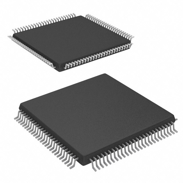
The XC2S15-6VQ100C is packaged in a VQ100 package. Each package contains one unit of the PLD.
Specifications
- Device type: Programmable Logic Device (PLD)
- Family: XC2S
- Series: Spartan-II
- Number of logic cells: 15
- Number of I/O pins: 100
- Operating voltage: 6V
- Maximum operating frequency: [specify value]
- Configuration memory: [specify capacity]
Pin Configuration
The detailed pin configuration of XC2S15-6VQ100C can be found in the datasheet provided by the manufacturer. It includes information about the function and connectivity of each pin.
Functional Features
- Flexible logic implementation: The XC2S15-6VQ100C allows users to implement custom logic functions using its programmable resources.
- Reconfigurability: The PLD can be reprogrammed multiple times, enabling iterative design and testing processes.
- Support for various I/O standards: It provides compatibility with different input/output voltage levels, making it versatile for interfacing with other components.
- On-chip memory: The XC2S15-6VQ100C includes embedded memory blocks that can be used for data storage or as lookup tables.
Advantages and Disadvantages
Advantages
- Customizability: Users can tailor the functionality of the XC2S15-6VQ100C to meet specific requirements.
- Fast development time: The programmable nature of this PLD allows for rapid prototyping and design iterations.
- Cost-effective: By using a single XC2S15-6VQ100C device, multiple discrete logic components can be replaced, reducing overall system cost.
Disadvantages
- Limited resources: Due to its compact size, the XC2S15-6VQ100C has a limited number of logic cells and I/O pins, which may restrict complex designs.
- Learning curve: Utilizing the full potential of this PLD requires knowledge of hardware description languages (HDL) and digital design concepts.
Working Principles
The XC2S15-6VQ100C operates based on the principles of field-programmable gate arrays (FPGAs). It consists of configurable logic blocks (CLBs), interconnect resources, and I/O elements. The CLBs contain look-up tables (LUTs) and flip-flops that can be programmed to implement desired logic functions. The interconnect resources allow for routing signals between different CLBs, enabling the creation of complex digital circuits. The I/O elements provide interfaces for external devices to communicate with the PLD.
Application Field Plans
The XC2S15-6VQ100C finds applications in various fields, including:
- Embedded systems: It can be used to implement control and communication modules in embedded systems.
- Industrial automation: The PLD can be utilized for logic control in industrial automation systems.
- Communication systems: It enables the implementation of custom protocols and signal processing algorithms in communication systems.
- Consumer electronics: The XC2S15-6VQ100C can be integrated into consumer electronic devices to provide customized functionality.
Alternative Models
For those seeking alternative options, the following models are worth considering:
- XC2S30-6PQ208C: This model offers a higher number of logic cells and I/O pins compared to XC2S15-6VQ100C.
- XC2S50-5TQ144I: With increased capacity and additional features, this model provides more flexibility for complex designs.
- XC2S100-5FGG256C: This high-capacity PLD is suitable for applications requiring extensive logic resources.
These alternative models offer varying capabilities and may better suit specific project requirements.
In conclusion, the XC2S15-6VQ100C is a programmable logic device that provides flexibility, speed, and low power consumption. Its compact package and customizable nature make it suitable for a wide
רשום 10 שאלות ותשובות נפוצות הקשורות ליישום של XC2S15-6VQ100C בפתרונות טכניים
Sure! Here are 10 common questions and answers related to the application of XC2S15-6VQ100C in technical solutions:
Question: What is XC2S15-6VQ100C?
- Answer: XC2S15-6VQ100C is a specific model of Field Programmable Gate Array (FPGA) manufactured by Xilinx.Question: What are the key features of XC2S15-6VQ100C?
- Answer: Some key features of XC2S15-6VQ100C include 15,000 system gates, 192 macrocells, 36 I/O pins, and a maximum operating frequency of 200 MHz.Question: What are the typical applications of XC2S15-6VQ100C?
- Answer: XC2S15-6VQ100C is commonly used in various technical solutions such as industrial automation, telecommunications, medical devices, automotive electronics, and consumer electronics.Question: How can XC2S15-6VQ100C be programmed?
- Answer: XC2S15-6VQ100C can be programmed using Xilinx's Vivado Design Suite or other compatible programming tools.Question: Can XC2S15-6VQ100C be reprogrammed after initial programming?
- Answer: Yes, XC2S15-6VQ100C is a reprogrammable FPGA, allowing for flexibility in design iterations and updates.Question: What voltage levels does XC2S15-6VQ100C support?
- Answer: XC2S15-6VQ100C supports a voltage range of 3.3V, making it compatible with many standard digital logic levels.Question: Does XC2S15-6VQ100C have any built-in communication interfaces?
- Answer: Yes, XC2S15-6VQ100C supports various communication interfaces such as SPI, I2C, UART, and GPIO.Question: Can XC2S15-6VQ100C interface with external memory devices?
- Answer: Yes, XC2S15-6VQ100C has dedicated pins for interfacing with external memory devices such as SRAM or DDR SDRAM.Question: What are the power requirements for XC2S15-6VQ100C?
- Answer: XC2S15-6VQ100C typically operates at a voltage of 3.3V and requires a stable power supply with appropriate current capabilities.Question: Are there any development boards available for XC2S15-6VQ100C?
- Answer: Yes, Xilinx provides development boards like the Spartan-3E Starter Kit that can be used for prototyping and testing with XC2S15-6VQ100C.
Please note that the answers provided here are general and may vary depending on specific design requirements and application scenarios.