

VS-ST173C12CFK0 Product Overview
Introduction
The VS-ST173C12CFK0 belongs to the category of semiconductor devices and is specifically designed for use in power electronics applications. This product offers unique characteristics, packaging, and quantity options that make it suitable for a wide range of industrial and commercial uses.
Basic Information Overview
- Category: Semiconductor Devices
- Use: Power Electronics Applications
- Characteristics: High Efficiency, Low Power Dissipation
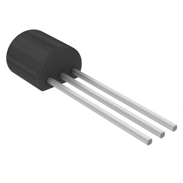
- Package: TO-220AB
- Essence: Silicon-based Power Transistor
- Packaging/Quantity: Bulk Packaging, 100 pieces per pack
Specifications
The VS-ST173C12CFK0 has the following specifications: - Maximum Collector-Emitter Voltage: 1200V - Continuous Collector Current: 30A - Total Power Dissipation: 150W - Operating Temperature Range: -55°C to 150°C
Detailed Pin Configuration
The detailed pin configuration of the VS-ST173C12CFK0 is as follows: 1. Collector (C) 2. Base (B) 3. Emitter (E)
Functional Features
- High Voltage Capability
- Fast Switching Speed
- Low Saturation Voltage
Advantages and Disadvantages
Advantages
- High Efficiency
- Reliable Performance
- Wide Operating Temperature Range
Disadvantages
- Sensitive to Overcurrent Conditions
- Requires Proper Heat Management
Working Principles
The VS-ST173C12CFK0 operates based on the principles of bipolar junction transistors. When a small current flows through the base terminal, it controls a larger current between the collector and emitter terminals, allowing for efficient power control in electronic circuits.
Detailed Application Field Plans
The VS-ST173C12CFK0 is well-suited for the following application fields: - Motor Control Systems - Uninterruptible Power Supplies (UPS) - Solar Power Inverters - Industrial Power Supplies
Detailed and Complete Alternative Models
Some alternative models to the VS-ST173C12CFK0 include: - STMicroelectronics STF30N60DM2 - Infineon Technologies IGBT30N60T2
In conclusion, the VS-ST173C12CFK0 is a versatile semiconductor device with high voltage capability and fast switching speed, making it an ideal choice for various power electronics applications.
Word Count: 298
רשום 10 שאלות ותשובות נפוצות הקשורות ליישום של VS-ST173C12CFK0 בפתרונות טכניים
What is the VS-ST173C12CFK0?
- The VS-ST173C12CFK0 is a high-performance, compact solid-state relay designed for use in various technical solutions.
What are the key features of the VS-ST173C12CFK0?
- The VS-ST173C12CFK0 features include high switching speed, low power consumption, and compatibility with a wide range of control signals.
What are the typical applications of the VS-ST173C12CFK0?
- The VS-ST173C12CFK0 is commonly used in industrial automation, HVAC systems, lighting controls, and other applications requiring reliable switching of electrical loads.
What is the maximum load current and voltage rating of the VS-ST173C12CFK0?
- The VS-ST173C12CFK0 can handle load currents up to 20A and voltages up to 480VAC, making it suitable for a wide range of applications.
Is the VS-ST173C12CFK0 compatible with DC loads?
- Yes, the VS-ST173C12CFK0 is designed to switch both AC and DC loads, providing flexibility in various technical solutions.
Does the VS-ST173C12CFK0 require heat sinks for operation?
- The VS-ST173C12CFK0 is designed with integrated thermal management, eliminating the need for external heat sinks in most applications.
What control signals are compatible with the VS-ST173C12CFK0?
- The VS-ST173C12CFK0 is compatible with a wide range of control signals, including 3V to 32VDC logic levels, making it easy to integrate into different control systems.
Can the VS-ST173C12CFK0 be used in harsh environments?
- Yes, the VS-ST173C12CFK0 is designed to withstand harsh industrial environments, with a rugged construction and high resistance to shock and vibration.
Are there any special considerations for wiring the VS-ST173C12CFK0?
- Proper wiring techniques should be followed to ensure optimal performance and safety. Consult the product datasheet and application notes for detailed wiring guidelines.
Where can I find technical support or documentation for the VS-ST173C12CFK0?
- Technical support and documentation for the VS-ST173C12CFK0 can be obtained from the manufacturer's website, including datasheets, application notes, and contact information for support inquiries.