

SN74LVTH126DGVR
Product Overview
- Category: Integrated Circuit (IC)
- Use: Logic Level Translator
- Characteristics: High-speed, low-voltage, and low-power consumption
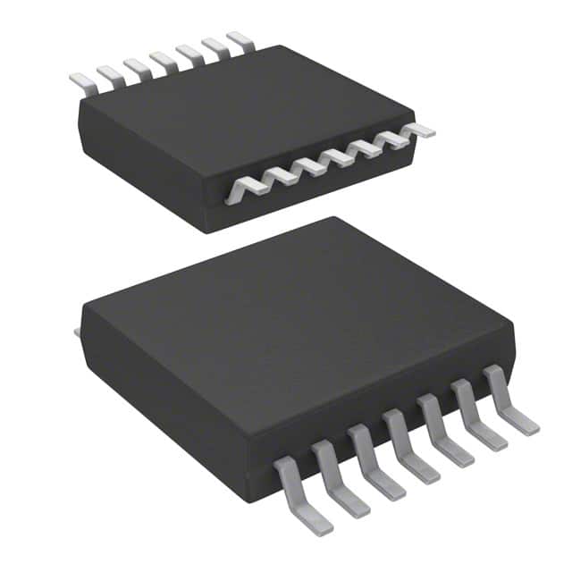
- Package: VSSOP (Very Small Outline Package)
- Essence: Translates signals between different voltage levels
- Packaging/Quantity: Tape and Reel, 2500 pieces per reel
Specifications
- Supply Voltage Range: 1.65V to 5.5V
- Input Voltage Range: 0V to VCC
- Output Voltage Range: 0V to VCC
- Maximum Operating Frequency: 400MHz
- Number of Channels: 4
- Input/Output Type: Tri-State
Detailed Pin Configuration
The SN74LVTH126DGVR has a total of 14 pins. The pin configuration is as follows:
- OE (Output Enable) - Active Low Output Enable
- A1 - Channel 1 Input
- Y1 - Channel 1 Output
- GND - Ground
- Y2 - Channel 2 Output
- A2 - Channel 2 Input
- VCC - Power Supply
- B1 - Channel 1 Input
- Y3 - Channel 3 Output
- A3 - Channel 3 Input
- B2 - Channel 2 Input
- Y4 - Channel 4 Output
- A4 - Channel 4 Input
- VCC - Power Supply
Functional Features
- Bidirectional voltage level translation between 1.65V and 5.5V
- Supports high-speed data transmission up to 400MHz
- Low power consumption for energy-efficient operation
- Tri-state outputs allow for easy bus sharing
- Robust design with ESD protection
Advantages and Disadvantages
Advantages: - Wide supply voltage range allows for compatibility with various systems - High-speed operation enables efficient data transfer - Low power consumption reduces energy usage - Tri-state outputs facilitate bus sharing in complex circuits - ESD protection ensures reliability in harsh environments
Disadvantages: - Limited number of channels (4) - Not suitable for voltage translation beyond the specified range
Working Principles
The SN74LVTH126DGVR is a logic level translator that enables communication between devices operating at different voltage levels. It utilizes a combination of MOSFETs and CMOS technology to achieve bidirectional voltage translation.
When the OE pin is low, the device is enabled, and the input signals on channels A1-A4 are translated to the corresponding output channels Y1-Y4. The translation is performed based on the voltage levels of the VCC and GND pins.
Detailed Application Field Plans
The SN74LVTH126DGVR finds applications in various fields where voltage level translation is required. Some of the common application areas include:
- Microcontrollers: Facilitates communication between microcontrollers operating at different voltage levels.
- Communication Systems: Enables signal translation between different voltage domains in communication systems.
- Industrial Automation: Used in industrial automation systems to interface between different voltage logic circuits.
- Consumer Electronics: Allows for voltage level translation in consumer electronic devices such as smartphones and tablets.
- Automotive Electronics: Used in automotive electronics to bridge the gap between different voltage domains.
Detailed and Complete Alternative Models
- SN74LVC1T45DBVR: Single-bit dual-supply voltage level translator with 3-state outputs.
- SN74AVC4T245PW: Quad-bit dual-supply voltage level translator with 3-state outputs.
- SN74LVC8T245PWR: Octal-bit dual-supply voltage level translator with 3-state outputs.
- SN74LVC2T45DCTRG4: Dual-bit dual-supply voltage level translator with 3-state outputs.
These alternative models offer similar functionality and can be considered as alternatives to the SN74LVTH126DGVR based on specific requirements.
In conclusion, the SN74LVTH126DGVR is a high-speed logic level translator IC that allows for bidirectional voltage translation between different voltage domains. Its low power consumption, wide supply voltage range, and tri-state outputs make it suitable for various applications in different fields.
רשום 10 שאלות ותשובות נפוצות הקשורות ליישום של SN74LVTH126DGVR בפתרונות טכניים
Sure! Here are 10 common questions and answers related to the application of SN74LVTH126DGVR:
Question: What is the SN74LVTH126DGVR?
Answer: The SN74LVTH126DGVR is a quad bus buffer gate with 3-state outputs, designed for low-voltage (3.3V) applications.Question: What is the maximum operating voltage for the SN74LVTH126DGVR?
Answer: The maximum operating voltage for this device is 3.6V.Question: What is the purpose of a bus buffer gate?
Answer: A bus buffer gate is used to isolate different sections of a circuit, allowing them to communicate without interfering with each other.Question: Can the SN74LVTH126DGVR be used in both input and output applications?
Answer: Yes, this device can be used as both an input buffer and an output driver.Question: What is the maximum output current that the SN74LVTH126DGVR can drive?
Answer: The maximum output current is typically 12mA.Question: Is the SN74LVTH126DGVR compatible with other logic families?
Answer: Yes, this device is compatible with both TTL and CMOS logic families.Question: What is the propagation delay of the SN74LVTH126DGVR?
Answer: The typical propagation delay is around 3.8ns.Question: Can the SN74LVTH126DGVR be used in high-speed applications?
Answer: Yes, this device is suitable for high-speed data transmission due to its low propagation delay and high-speed operation.Question: Does the SN74LVTH126DGVR have internal pull-up or pull-down resistors?
Answer: No, this device does not have internal pull-up or pull-down resistors.Question: What is the package type for the SN74LVTH126DGVR?
Answer: The SN74LVTH126DGVR is available in a small SOT-23-5 package.
Please note that these answers are general and may vary depending on specific datasheet specifications and application requirements.