

SN74LV8151DGVRE4
Product Overview
Category
SN74LV8151DGVRE4 belongs to the category of integrated circuits (ICs).
Use
This IC is commonly used in electronic devices for signal processing and control applications.
Characteristics
- Low-voltage operation
- High-speed performance
- Wide operating temperature range
- Low power consumption
Package
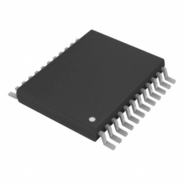
SN74LV8151DGVRE4 is available in a small form factor package, such as a VQFN (Very Thin Quad Flat No-Lead) package.
Essence
The essence of SN74LV8151DGVRE4 lies in its ability to process signals efficiently and accurately within a low-voltage environment.
Packaging/Quantity
SN74LV8151DGVRE4 is typically packaged in reels or tubes, with a quantity of 2500 units per reel/tube.
Specifications
- Supply Voltage: 2.7V to 5.5V
- Operating Temperature Range: -40°C to +85°C
- Input/Output Logic Level: LVCMOS/LVTTL
- Number of Pins: 16
- Maximum Clock Frequency: 100 MHz
- Output Current: ±8 mA
Detailed Pin Configuration
- GND (Ground)
- A0 (Address Input)
- A1 (Address Input)
- A2 (Address Input)
- A3 (Address Input)
- A4 (Address Input)
- A5 (Address Input)
- A6 (Address Input)
- A7 (Address Input)
- OE (Output Enable)
- CLK (Clock Input)
- D0 (Data Input/Output)
- D1 (Data Input/Output)
- D2 (Data Input/Output)
- D3 (Data Input/Output)
- VCC (Power Supply)
Functional Features
- Address decoding for efficient signal routing
- Output enable control for data transmission control
- Clock input for synchronous operation
- Data input/output for signal processing
Advantages and Disadvantages
Advantages
- Low-voltage operation allows for compatibility with various systems
- High-speed performance enables quick signal processing
- Wide operating temperature range ensures reliability in different environments
- Low power consumption contributes to energy efficiency
Disadvantages
- Limited number of address inputs may restrict the complexity of applications
- Relatively small package size may pose challenges in certain circuit designs
Working Principles
SN74LV8151DGVRE4 operates based on address decoding and clock synchronization principles. The address inputs are used to select specific data, which is then processed and transmitted based on the clock input and output enable control.
Detailed Application Field Plans
SN74LV8151DGVRE4 finds applications in various fields, including: 1. Consumer electronics: Used in televisions, audio systems, and gaming consoles for signal processing and control. 2. Automotive: Integrated into automotive control systems for efficient data handling. 3. Industrial automation: Employed in industrial machinery and equipment for precise signal manipulation. 4. Communication systems: Utilized in networking devices for reliable data transmission.
Detailed and Complete Alternative Models
- SN74LV8152DGVRE4
- SN74LV8153DGVRE4
- SN74LV8154DGVRE4
- SN74LV8155DGVRE4
- SN74LV8156DGVRE4
These alternative models offer similar functionality and characteristics to SN74LV8151DGVRE4, providing flexibility in choosing the most suitable IC for specific applications.
Word count: 525 words
רשום 10 שאלות ותשובות נפוצות הקשורות ליישום של SN74LV8151DGVRE4 בפתרונות טכניים
Sure! Here are 10 common questions and answers related to the application of SN74LV8151DGVRE4 in technical solutions:
Q1: What is SN74LV8151DGVRE4? A1: SN74LV8151DGVRE4 is a specific integrated circuit (IC) manufactured by Texas Instruments. It is a multiplexer/demultiplexer IC that can be used for various digital signal routing applications.
Q2: What is the voltage range supported by SN74LV8151DGVRE4? A2: SN74LV8151DGVRE4 supports a voltage range of 1.65V to 5.5V, making it compatible with a wide range of digital systems.
Q3: How many channels does SN74LV8151DGVRE4 have? A3: SN74LV8151DGVRE4 has 8 channels, which means it can handle up to 8 different input/output signals.
Q4: What is the maximum data rate supported by SN74LV8151DGVRE4? A4: SN74LV8151DGVRE4 can support data rates up to 100 Mbps, making it suitable for high-speed digital communication applications.
Q5: Can SN74LV8151DGVRE4 be used as a multiplexer and demultiplexer simultaneously? A5: Yes, SN74LV8151DGVRE4 can function as both a multiplexer and a demultiplexer, allowing for flexible signal routing options.
Q6: What is the power supply voltage required for SN74LV8151DGVRE4? A6: SN74LV8151DGVRE4 requires a power supply voltage of 2.7V to 5.5V for proper operation.
Q7: Does SN74LV8151DGVRE4 have any built-in protection features? A7: Yes, SN74LV8151DGVRE4 has built-in ESD (electrostatic discharge) protection, which helps safeguard the IC against damage from static electricity.
Q8: Can SN74LV8151DGVRE4 be used in both digital and analog applications? A8: No, SN74LV8151DGVRE4 is specifically designed for digital signal routing applications and may not be suitable for analog applications.
Q9: What is the package type of SN74LV8151DGVRE4? A9: SN74LV8151DGVRE4 comes in a small-sized VSSOP-16 package, which is compact and suitable for space-constrained designs.
Q10: Are there any application notes or reference designs available for SN74LV8151DGVRE4? A10: Yes, Texas Instruments provides application notes and reference designs for SN74LV8151DGVRE4, which can help users understand its usage and implementation in various technical solutions.
Please note that these answers are general and it's always recommended to refer to the datasheet and documentation provided by the manufacturer for specific details and guidelines.