

SN74FB2041ARCG3
Product Overview
- Category: Integrated Circuit (IC)
- Use: Logic Gate
- Characteristics: High-speed, low-power consumption
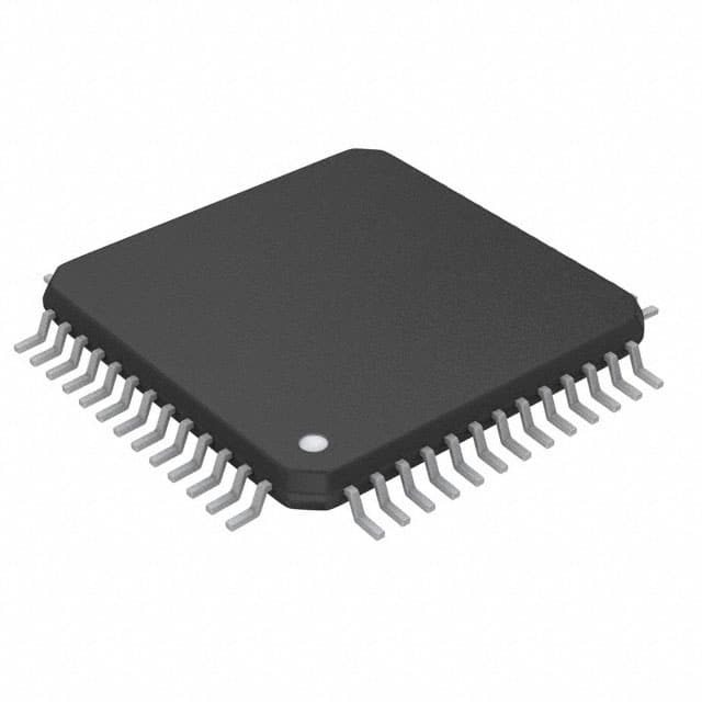
- Package: 20-pin QFN (Quad Flat No-Lead)
- Essence: Digital logic gate with four inputs and one output
- Packaging/Quantity: Tape and Reel, 2500 units per reel
Specifications
- Supply Voltage: 2.7V to 3.6V
- Input Voltage: 0V to VCC
- Output Voltage: 0V to VCC
- Operating Temperature Range: -40°C to +85°C
- Propagation Delay: 2.5ns (typical)
- Maximum Frequency: 200MHz
Detailed Pin Configuration
The SN74FB2041ARCG3 has a total of 20 pins. The pin configuration is as follows:
- A1 - Input A1
- B1 - Input B1
- C1 - Input C1
- D1 - Input D1
- GND - Ground
- Y - Output Y
- D2 - Input D2
- C2 - Input C2
- B2 - Input B2
- A2 - Input A2
- VCC - Power Supply
- NC - No Connection
- NC - No Connection
- NC - No Connection
- NC - No Connection
- NC - No Connection
- NC - No Connection
- NC - No Connection
- NC - No Connection
- NC - No Connection
Functional Features
The SN74FB2041ARCG3 is a quad-input AND gate that performs logical AND operations on its four input signals (A1, B1, C1, D1) and provides the output signal (Y). It operates at high speed and consumes low power, making it suitable for various digital logic applications.
Advantages and Disadvantages
Advantages: - High-speed operation - Low power consumption - Compact package size - Wide operating temperature range
Disadvantages: - Limited number of inputs (four) - Not suitable for complex logic operations
Working Principles
The SN74FB2041ARCG3 uses CMOS technology to implement the logical AND operation. When all four input signals are high (logic level 1), the output signal is also high. If any of the input signals is low (logic level 0), the output signal becomes low. The propagation delay is minimal, ensuring fast response times.
Detailed Application Field Plans
The SN74FB2041ARCG3 can be used in various applications that require logical AND operations with multiple inputs. Some potential application fields include:
- Digital signal processing
- Data communication systems
- Microcontroller-based systems
- Industrial automation
- Robotics
Detailed and Complete Alternative Models
- SN74FB2041ARGYR - 20-pin QFN package, reel packaging, 2500 units per reel
- SN74FB2041ARHBR - 20-pin VQFN (Very Thin Quad Flat No-Lead) package, tape and reel packaging, 3000 units per reel
- SN74FB2041ARHBRR - 20-pin VQFN package, reel packaging, 3000 units per reel
- SN74FB2041ARHBT - 20-pin VQFN package, tube packaging, 98 units per tube
These alternative models offer similar functionality and characteristics to the SN74FB2041ARCG3, providing flexibility in choosing the most suitable option for specific requirements.
Word count: 346 words
רשום 10 שאלות ותשובות נפוצות הקשורות ליישום של SN74FB2041ARCG3 בפתרונות טכניים
Sure! Here are 10 common questions and answers related to the application of SN74FB2041ARCG3 in technical solutions:
Q1: What is SN74FB2041ARCG3? A1: SN74FB2041ARCG3 is a specific model of integrated circuit (IC) manufactured by Texas Instruments. It is a quad bus buffer with 3-state outputs.
Q2: What is the purpose of SN74FB2041ARCG3? A2: The purpose of SN74FB2041ARCG3 is to provide buffering and signal isolation for digital signals in various electronic systems.
Q3: What voltage levels does SN74FB2041ARCG3 support? A3: SN74FB2041ARCG3 supports voltage levels ranging from 2V to 5.5V, making it compatible with a wide range of digital systems.
Q4: How many inputs and outputs does SN74FB2041ARCG3 have? A4: SN74FB2041ARCG3 has four inputs and four outputs, making it a quad buffer.
Q5: Can SN74FB2041ARCG3 handle bidirectional data flow? A5: No, SN74FB2041ARCG3 is a unidirectional buffer, meaning it can only buffer signals in one direction.
Q6: What is the maximum operating frequency of SN74FB2041ARCG3? A6: SN74FB2041ARCG3 has a maximum operating frequency of 100 MHz, allowing it to handle high-speed digital signals.
Q7: Does SN74FB2041ARCG3 have any built-in protection features? A7: Yes, SN74FB2041ARCG3 has built-in ESD (electrostatic discharge) protection, which helps safeguard against damage from static electricity.
Q8: Can SN74FB2041ARCG3 be used in automotive applications? A8: Yes, SN74FB2041ARCG3 is qualified for automotive applications and can operate within the specified temperature range for automotive environments.
Q9: What is the power supply voltage range for SN74FB2041ARCG3? A9: SN74FB2041ARCG3 operates with a power supply voltage range of 2V to 5.5V.
Q10: Are there any recommended application circuits available for SN74FB2041ARCG3? A10: Yes, Texas Instruments provides application notes and reference designs that showcase recommended circuit configurations for using SN74FB2041ARCG3 in various technical solutions.
Please note that these answers are general and may vary depending on the specific requirements and use cases. It's always recommended to refer to the datasheet and documentation provided by the manufacturer for accurate and detailed information.