

SN74AUP2G241YFPR
Product Overview
Category
SN74AUP2G241YFPR belongs to the category of integrated circuits (ICs).
Use
This product is commonly used in electronic devices for signal amplification and switching purposes.
Characteristics
- Low power consumption
- High-speed operation
- Wide operating voltage range
- Small package size
- RoHS compliant
Package
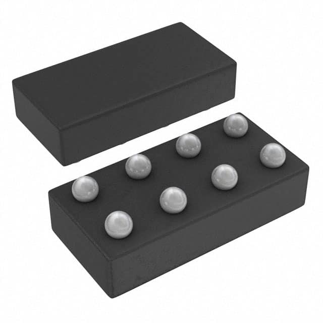
SN74AUP2G241YFPR is available in a small form factor package, such as a flip-chip package or a leadless package.
Essence
The essence of SN74AUP2G241YFPR lies in its ability to amplify and switch signals efficiently while consuming minimal power.
Packaging/Quantity
This product is typically packaged in reels or trays, with a quantity of 3000 units per reel/tray.
Specifications
- Supply Voltage: 1.65V to 3.6V
- Operating Temperature Range: -40°C to +85°C
- Input Voltage Range: 0V to VCC
- Output Voltage Range: 0V to VCC
- Maximum Propagation Delay: 4.5ns
- Maximum Quiescent Current: 10μA
Detailed Pin Configuration
SN74AUP2G241YFPR consists of the following pins:
- A Input 1
- B Input 1
- Y Output 1
- GND (Ground)
- Y Output 2
- B Input 2
- A Input 2
- VCC (Supply Voltage)
Functional Features
- Dual 2-input NOR gate functionality
- High-speed operation for efficient signal processing
- Low power consumption for energy-efficient applications
- Wide operating voltage range allows compatibility with various systems
Advantages and Disadvantages
Advantages
- Low power consumption makes it suitable for battery-powered devices
- High-speed operation enables quick signal processing
- Wide operating voltage range provides flexibility in system integration
- Small package size saves board space
Disadvantages
- Limited number of inputs and outputs restricts its application in complex circuits
- Propagation delay may affect timing-sensitive applications
Working Principles
SN74AUP2G241YFPR operates based on the principles of NOR gate logic. It takes two input signals and produces an output signal based on the logical NOR operation.
Detailed Application Field Plans
SN74AUP2G241YFPR finds applications in various electronic devices, including but not limited to: - Mobile phones - Tablets - Digital cameras - Portable gaming consoles - Wearable devices
Detailed and Complete Alternative Models
Some alternative models that can be considered as alternatives to SN74AUP2G241YFPR are: - SN74AUP1G241 - SN74LVC2G241 - SN74LV2G241
These models offer similar functionality and characteristics, providing options for different design requirements.
Word count: 346 words
רשום 10 שאלות ותשובות נפוצות הקשורות ליישום של SN74AUP2G241YFPR בפתרונות טכניים
Sure! Here are 10 common questions and answers related to the application of SN74AUP2G241YFPR in technical solutions:
Q: What is SN74AUP2G241YFPR? A: SN74AUP2G241YFPR is a dual buffer/driver IC (integrated circuit) designed for voltage level translation applications.
Q: What is the voltage range supported by SN74AUP2G241YFPR? A: SN74AUP2G241YFPR supports voltage translation from 0.8V to 3.6V.
Q: Can SN74AUP2G241YFPR be used for bidirectional level translation? A: No, SN74AUP2G241YFPR is a unidirectional buffer/driver and does not support bidirectional level translation.
Q: What is the maximum output current of SN74AUP2G241YFPR? A: The maximum output current of SN74AUP2G241YFPR is typically 24mA.
Q: Is SN74AUP2G241YFPR suitable for high-speed applications? A: Yes, SN74AUP2G241YFPR is designed for high-speed operation and can be used in applications with fast switching requirements.
Q: Can SN74AUP2G241YFPR be used in automotive applications? A: Yes, SN74AUP2G241YFPR is qualified for automotive applications and meets the necessary standards.
Q: Does SN74AUP2G241YFPR have built-in ESD protection? A: Yes, SN74AUP2G241YFPR has built-in ESD (electrostatic discharge) protection to safeguard against electrostatic damage.
Q: What is the package type of SN74AUP2G241YFPR? A: SN74AUP2G241YFPR is available in a small footprint 8-pin DSBGA (MicroStar Junior™) package.
Q: Can SN74AUP2G241YFPR be used with different supply voltages for input and output sides? A: Yes, SN74AUP2G241YFPR supports voltage translation between different supply voltages on the input and output sides.
Q: Are there any application notes or reference designs available for SN74AUP2G241YFPR? A: Yes, Texas Instruments provides application notes and reference designs that can help in implementing SN74AUP2G241YFPR in various technical solutions.
Please note that the answers provided here are general and may vary based on specific datasheet and application requirements. It's always recommended to refer to the official documentation and consult with technical experts for accurate information.