

CSD95491Q5MC - English Editing Encyclopedia Entry
Product Overview
Category
CSD95491Q5MC belongs to the category of integrated circuits (ICs).
Use
This IC is commonly used in electronic devices for power management and control.
Characteristics
- High efficiency
- Low power consumption
- Compact size
- Wide operating voltage range
Package
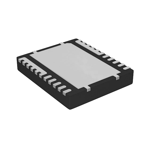
CSD95491Q5MC is available in a small outline package (SOP) or a quad flat no-leads package (QFN).
Essence
The essence of CSD95491Q5MC lies in its ability to efficiently manage and control power in electronic devices, ensuring optimal performance and energy conservation.
Packaging/Quantity
The IC is typically packaged in reels or trays, with quantities varying based on customer requirements.
Specifications
- Input Voltage Range: 2.7V to 5.5V
- Output Voltage Range: 0.6V to 3.3V
- Maximum Output Current: 1A
- Operating Temperature Range: -40°C to 85°C
- Switching Frequency: 1.2MHz
Detailed Pin Configuration
CSD95491Q5MC features a total of 16 pins, each serving a specific function. The pin configuration is as follows:
- VIN: Input voltage pin
- GND: Ground pin
- EN: Enable pin
- FB: Feedback pin
- VOUT: Output voltage pin
- SW: Switching pin
- PGND: Power ground pin
- AGND: Analog ground pin
- COMP: Compensation pin
- SS/TR: Soft-start/Tracking pin
- PG: Power good pin
- BST: Bootstrap pin
- LX1: Inductor connection pin 1
- LX2: Inductor connection pin 2
- VDD: Supply voltage pin
- PGND: Power ground pin
Functional Features
- High-efficiency synchronous buck converter
- Integrated power MOSFETs for reduced external components
- Adjustable output voltage through feedback pin
- Soft-start and tracking functionality for controlled startup
- Overcurrent protection and thermal shutdown features
Advantages and Disadvantages
Advantages
- High efficiency leads to energy savings
- Compact size allows for space-efficient designs
- Wide operating voltage range enables compatibility with various devices
- Integrated power MOSFETs reduce the need for external components
Disadvantages
- Limited maximum output current of 1A
- Operating temperature range may not be suitable for extreme environments
Working Principles
CSD95491Q5MC operates as a synchronous buck converter, converting the input voltage to a lower output voltage with high efficiency. The integrated power MOSFETs handle the switching operation, while the feedback mechanism adjusts the output voltage based on the desired level. The soft-start feature ensures a controlled startup, while overcurrent protection and thermal shutdown mechanisms safeguard against potential damage.
Detailed Application Field Plans
CSD95491Q5MC finds applications in various electronic devices, including but not limited to: - Mobile phones - Tablets - Portable gaming consoles - Wearable devices - IoT devices
Detailed and Complete Alternative Models
Some alternative models that offer similar functionality to CSD95491Q5MC include: - CSD95372Q5M - TPS54332 - LTC3633 - MP2307
These alternatives can be considered based on specific requirements and design considerations.
Word count: 450 words
רשום 10 שאלות ותשובות נפוצות הקשורות ליישום של CSD95491Q5MC בפתרונות טכניים
Sure! Here are 10 common questions and answers related to the application of CSD95491Q5MC in technical solutions:
Question: What is CSD95491Q5MC?
Answer: CSD95491Q5MC is a specific model of integrated circuit (IC) designed for power management applications.Question: What are the key features of CSD95491Q5MC?
Answer: Some key features of CSD95491Q5MC include high efficiency, low quiescent current, overcurrent protection, and thermal shutdown.Question: What are the typical applications of CSD95491Q5MC?
Answer: CSD95491Q5MC is commonly used in various technical solutions such as battery-powered devices, portable electronics, IoT devices, and industrial automation systems.Question: How does CSD95491Q5MC help in power management?
Answer: CSD95491Q5MC provides efficient power conversion and regulation, ensuring stable and reliable power supply to different components of a system.Question: What is the input voltage range supported by CSD95491Q5MC?
Answer: The input voltage range of CSD95491Q5MC typically varies from 2.7V to 5.5V, making it suitable for a wide range of applications.Question: Can CSD95491Q5MC handle multiple output voltages?
Answer: Yes, CSD95491Q5MC can support multiple output voltages, allowing it to power different components with varying voltage requirements.Question: Does CSD95491Q5MC have built-in protection features?
Answer: Yes, CSD95491Q5MC incorporates overcurrent protection and thermal shutdown mechanisms to safeguard against potential damage or overheating.Question: What is the efficiency of CSD95491Q5MC?
Answer: CSD95491Q5MC offers high efficiency, typically above 90%, ensuring minimal power loss during the conversion process.Question: Can CSD95491Q5MC operate in a wide temperature range?
Answer: Yes, CSD95491Q5MC is designed to operate reliably in a wide temperature range, making it suitable for various environmental conditions.Question: Are there any application notes or reference designs available for CSD95491Q5MC?
Answer: Yes, the manufacturer of CSD95491Q5MC provides application notes and reference designs that can help engineers in implementing the IC effectively in their technical solutions.
Please note that the answers provided here are general and may vary depending on the specific datasheet and documentation provided by the manufacturer of CSD95491Q5MC.