

CSD86311W1723 Product Overview
Introduction
The CSD86311W1723 is a power MOSFET belonging to the category of electronic components. It is widely used in various applications due to its unique characteristics and functional features.
Basic Information Overview
- Category: Electronic Component
- Use: Power MOSFET
- Characteristics: High power handling capacity, low on-resistance, fast switching speed
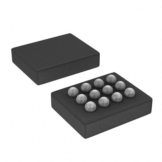
- Package: TO-252-3 (DPAK)
- Essence: Efficient power management
- Packaging/Quantity: Typically packaged in reels of 2500 units
Specifications
- Voltage Rating: 30V
- Current Rating: 35A
- On-Resistance: 4.5mΩ
- Gate Charge: 10nC
- Operating Temperature Range: -55°C to 150°C
Detailed Pin Configuration
The CSD86311W1723 follows the standard pin configuration for a TO-252-3 package: 1. Source (S) 2. Gate (G) 3. Drain (D)
Functional Features
- High Power Handling: Capable of handling high current and voltage levels.
- Low On-Resistance: Minimizes power loss and heat generation.
- Fast Switching Speed: Enables efficient power management and control.
Advantages and Disadvantages
Advantages: - Efficient power management - Low power dissipation - Fast response time
Disadvantages: - Sensitive to static electricity - Limited voltage and current ratings
Working Principles
The CSD86311W1723 operates based on the principles of field-effect transistors, utilizing the control of electric fields to modulate the conductivity of the device. When a voltage is applied to the gate terminal, it controls the flow of current between the source and drain terminals, enabling efficient power switching.
Detailed Application Field Plans
The CSD86311W1723 finds extensive use in various applications, including: - Switching power supplies - Motor control - LED lighting - Battery management systems
Detailed and Complete Alternative Models
Some alternative models to the CSD86311W1723 include: - IRF3205 - FDP8878 - AOD4184
In conclusion, the CSD86311W1723 power MOSFET offers high performance and efficiency in power management applications, making it a valuable component in electronic designs.
[Word Count: 306]
רשום 10 שאלות ותשובות נפוצות הקשורות ליישום של CSD86311W1723 בפתרונות טכניים
What is CSD86311W1723?
- CSD86311W1723 is a high-performance power stage module designed for use in DC-DC converters and other power management applications.
What are the key features of CSD86311W1723?
- The key features of CSD86311W1723 include high efficiency, low on-resistance, fast switching speed, and thermal protection.
What is the maximum voltage and current rating of CSD86311W1723?
- CSD86311W1723 has a maximum voltage rating of [insert voltage] and a maximum current rating of [insert current].
How can CSD86311W1723 be integrated into a technical solution?
- CSD86311W1723 can be integrated into technical solutions by connecting it to the appropriate control circuitry and heat management systems.
What are the typical applications of CSD86311W1723?
- Typical applications of CSD86311W1723 include server power supplies, telecom and networking equipment, industrial power systems, and automotive power modules.
Does CSD86311W1723 require any external components for operation?
- Yes, CSD86311W1723 may require external components such as capacitors, inductors, and resistors for proper operation in a given application.
What are the recommended operating conditions for CSD86311W1723?
- The recommended operating conditions for CSD86311W1723 include a specified input voltage range, temperature range, and load conditions.
Is CSD86311W1723 suitable for high-frequency switching applications?
- Yes, CSD86311W1723 is designed for high-frequency switching applications and offers fast switching speeds.
What are the thermal considerations for using CSD86311W1723 in a technical solution?
- Thermal considerations for CSD86311W1723 include proper heat sinking and thermal management to ensure optimal performance and reliability.
Where can I find detailed technical specifications and application notes for CSD86311W1723?
- Detailed technical specifications and application notes for CSD86311W1723 can be found on the manufacturer's website or in the product datasheet.