

74LVTH18511DGGRE4
Basic Information Overview
- Category: Integrated Circuit (IC)
- Use: Logic Level Translator
- Characteristics: High-speed, low-power, voltage-level shifting
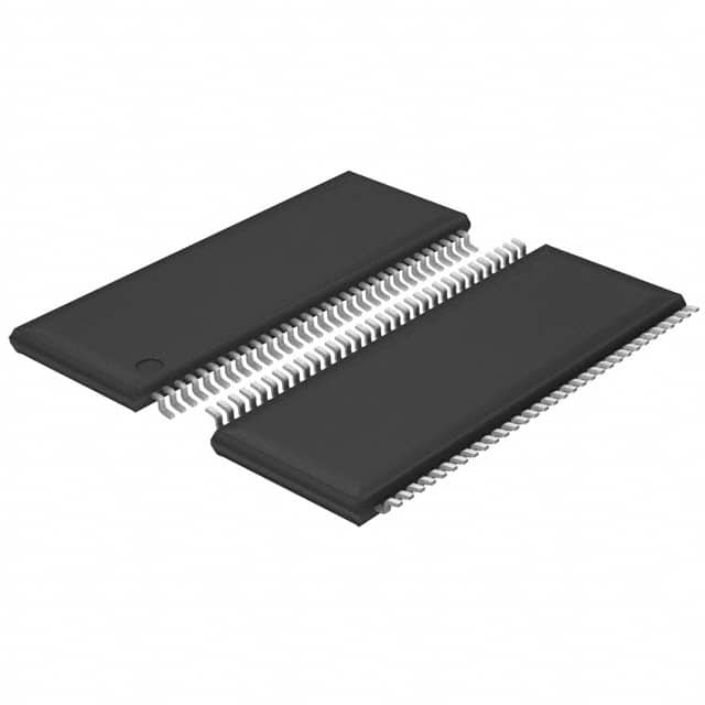
- Package: TSSOP (Thin Shrink Small Outline Package)
- Essence: Translates logic levels between different voltage domains
- Packaging/Quantity: Tape and Reel, 2500 pieces per reel
Specifications
- Supply Voltage Range: 1.65V to 5.5V
- Logic Family: LVTH
- Number of Channels: 18
- Input/Output Type: Non-Inverting
- Propagation Delay: 2.3ns (typical)
- Operating Temperature Range: -40°C to +85°C
Detailed Pin Configuration
The 74LVTH18511DGGRE4 IC has a total of 56 pins arranged in a specific configuration. The pinout diagram is as follows:
___________
      |           |
   A1 |1         56| VCC
   B1 |2         55| GND
   Y1 |3         54| A2
   Y2 |4         53| B2
   Y3 |5         52| A3
   Y4 |6         51| B3
   Y5 |7         50| A4
   Y6 |8         49| B4
   Y7 |9         48| A5
   Y8 |10        47| B5
   Y9 |11        46| A6
  Y10 |12        45| B6
  Y11 |13        44| A7
  Y12 |14        43| B7
  Y13 |15        42| A8
  Y14 |16        41| B8
  Y15 |17        40| A9
  Y16 |18        39| B9
  Y17 |19        38| A10
  Y18 |20        37| B10
   G1 |21        36| A11
   G2 |22        35| B11
   G3 |23        34| A12
   G4 |24        33| B12
   G5 |25        32| A13
   G6 |26        31| B13
   G7 |27        30| A14
   G8 |28        29| B14
      |___________|
Functional Features
- Logic Level Translation: The IC allows for bidirectional voltage-level shifting between different logic families, enabling seamless communication between devices operating at different voltage levels.
- High-Speed Operation: The 74LVTH18511DGGRE4 offers fast propagation delay, making it suitable for applications requiring quick signal transmission.
- Low Power Consumption: The IC is designed to consume minimal power, enhancing energy efficiency in electronic systems.
Advantages and Disadvantages
Advantages: - Wide supply voltage range allows compatibility with various systems. - Non-inverting input/output configuration simplifies circuit design. - High-speed operation enables efficient data transfer.
Disadvantages: - Limited number of channels may restrict its use in complex systems. - Temperature range might not be suitable for extreme environments.
Working Principles
The 74LVTH18511DGGRE4 utilizes a combination of MOSFETs and CMOS technology to achieve logic level translation. It employs a voltage divider network and level-shifting circuitry to convert signals from one voltage domain to another while maintaining signal integrity.
Detailed Application Field Plans
The 74LVTH18511DGGRE4 is commonly used in various applications, including: 1. Microcontroller interfacing: It facilitates communication between microcontrollers operating at different voltage levels. 2. Sensor networks: The IC enables level translation between sensors and microcontrollers, ensuring compatibility in mixed-voltage environments. 3. Industrial automation: It finds application in control systems where different components operate at distinct voltage levels.
Detailed and Complete Alternative Models
- SN74LVC1T45DBVR: Single-bit dual-supply bus transceiver with voltage-level translation capability.
- TXB0108PWR: Eight-channel bidirectional voltage-level translator with automatic direction sensing.
- PCA9306DCUR: Dual bidirectional I2C-bus and SMBus voltage-level translator.
These alternative models offer similar functionality and can be considered as substitutes for the 74LVTH18511DGGRE4 in specific applications.
Word count: 518 words
רשום 10 שאלות ותשובות נפוצות הקשורות ליישום של 74LVTH18511DGGRE4 בפתרונות טכניים
Sure! Here are 10 common questions and answers related to the application of 74LVTH18511DGGRE4 in technical solutions:
Q: What is the 74LVTH18511DGGRE4? A: The 74LVTH18511DGGRE4 is a 18-bit universal bus driver with 3-state outputs, designed for low-voltage (3.3V) applications.
Q: What is the purpose of the 74LVTH18511DGGRE4? A: The purpose of this IC is to provide bidirectional buffering between a high-speed bus and a low-speed or wide bus.
Q: What is the maximum operating voltage for the 74LVTH18511DGGRE4? A: The maximum operating voltage for this IC is 3.6V.
Q: Can the 74LVTH18511DGGRE4 be used in both input and output applications? A: Yes, this IC can be used as both an input buffer and an output driver.
Q: What is the maximum data rate supported by the 74LVTH18511DGGRE4? A: The maximum data rate supported by this IC is typically 400Mbps.
Q: Does the 74LVTH18511DGGRE4 have internal pull-up or pull-down resistors? A: No, this IC does not have internal pull-up or pull-down resistors.
Q: Can the 74LVTH18511DGGRE4 be used in automotive applications? A: Yes, this IC is suitable for automotive applications as it meets the AEC-Q100 standard.
Q: What is the power supply range for the 74LVTH18511DGGRE4? A: The power supply range for this IC is typically 2.7V to 3.6V.
Q: Does the 74LVTH18511DGGRE4 have overvoltage protection? A: No, this IC does not have built-in overvoltage protection. External measures should be taken to prevent overvoltage.
Q: What package options are available for the 74LVTH18511DGGRE4? A: This IC is available in a TSSOP-56 package.
Please note that these answers are general and may vary depending on the specific datasheet and manufacturer's specifications for the 74LVTH18511DGGRE4.