

TSM6866SDCA RVG
Introduction
The TSM6866SDCA RVG is a semiconductor device belonging to the category of voltage regulators. This entry provides an overview of its basic information, specifications, detailed pin configuration, functional features, advantages and disadvantages, working principles, detailed application field plans, and alternative models.
Basic Information Overview
- Category: Voltage Regulator
- Use: Regulating voltage in electronic circuits
- Characteristics: High precision, low dropout voltage, low quiescent current
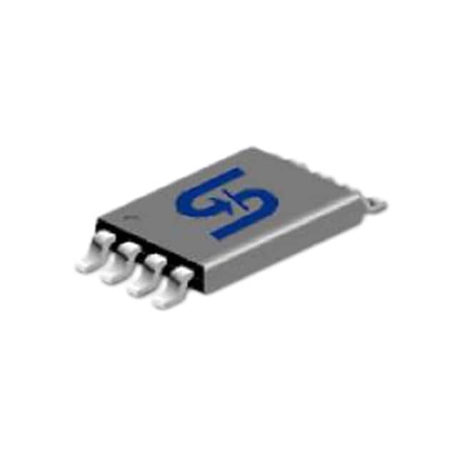
- Package: Small outline package (SOP)
- Essence: Efficient voltage regulation for electronic devices
- Packaging/Quantity: Typically available in reels of 2500 units
Specifications
- Input Voltage Range: 2.5V to 6.0V
- Output Voltage Range: 1.2V to 5.5V
- Output Current: Up to 1.5A
- Dropout Voltage: 200mV at 1A
- Quiescent Current: 75µA
- Operating Temperature Range: -40°C to 125°C
Detailed Pin Configuration
The TSM6866SDCA RVG has a standard 5-pin configuration: 1. VIN (Input Voltage) 2. GND (Ground) 3. EN (Enable) 4. NC (No Connection) 5. VOUT (Output Voltage)
Functional Features
- Low Dropout Voltage: Ensures stable output even with small input-output differentials
- Current Limit Protection: Safeguards the regulator and load against overcurrent conditions
- Thermal Shutdown: Protects the device from overheating
- Enable Function: Allows for external control of the regulator's operation
Advantages and Disadvantages
Advantages
- High precision voltage regulation
- Low dropout voltage for efficient power conversion
- Compact SOP package for space-constrained applications
Disadvantages
- Limited maximum output current compared to some competing models
- Narrower input voltage range
Working Principles
The TSM6866SDCA RVG operates by comparing the output voltage to a reference voltage and adjusting the pass element to maintain a stable output. It utilizes feedback control to regulate the output voltage despite variations in input voltage and load conditions.
Detailed Application Field Plans
The TSM6866SDCA RVG is well-suited for various portable and battery-powered applications, including: - Mobile phones - Portable media players - Handheld gaming devices - Wearable electronics
Detailed and Complete Alternative Models
Some alternative models to the TSM6866SDCA RVG include: - LM1117 - XC6206 - AP2112
In conclusion, the TSM6866SDCA RVG offers high precision voltage regulation in a compact package, making it suitable for a wide range of portable electronic devices.
Word Count: 398
רשום 10 שאלות ותשובות נפוצות הקשורות ליישום של TSM6866SDCA RVG בפתרונות טכניים
What is TSM6866SDCA RVG?
- TSM6866SDCA RVG is a high-performance CMOS image sensor designed for use in digital radiography applications, particularly in dental and medical imaging.
What are the key features of TSM6866SDCA RVG?
- The key features include high resolution, low noise, wide dynamic range, and fast readout speed, making it suitable for capturing detailed X-ray images with excellent clarity.
How does TSM6866SDCA RVG contribute to technical solutions in dental imaging?
- TSM6866SDCA RVG enables dentists to capture high-quality intraoral X-ray images, facilitating accurate diagnosis and treatment planning.
Can TSM6866SDCA RVG be integrated into existing dental imaging systems?
- Yes, TSM6866SDCA RVG is designed for easy integration into various dental imaging systems, offering compatibility with standard interfaces and protocols.
What are the advantages of using TSM6866SDCA RVG in medical imaging applications?
- TSM6866SDCA RVG offers superior image quality, enhanced diagnostic capabilities, and efficient workflow in medical imaging, contributing to improved patient care.
Is TSM6866SDCA RVG suitable for use in portable X-ray devices?
- Yes, TSM6866SDCA RVG's compact size and low power consumption make it well-suited for integration into portable X-ray devices, enabling point-of-care imaging solutions.
How does TSM6866SDCA RVG address the need for radiation dose reduction in X-ray imaging?
- TSM6866SDCA RVG's sensitivity and dynamic range allow for the capture of high-quality images at lower radiation doses, supporting the trend towards minimizing patient exposure.
Can TSM6866SDCA RVG support real-time imaging applications?
- Yes, TSM6866SDCA RVG's fast readout speed and low latency enable real-time imaging for applications such as fluoroscopy and dynamic radiography.
What type of image processing and enhancement capabilities does TSM6866SDCA RVG offer?
- TSM6866SDCA RVG provides raw image data that can be processed and enhanced using advanced algorithms to optimize image quality and diagnostic information.
Are there any specific installation or calibration requirements for TSM6866SDCA RVG?
- TSM6866SDCA RVG is designed for straightforward installation and typically requires minimal calibration, ensuring ease of integration into technical solutions.