

SI5335D-B03977-GM
Basic Information Overview
- Category: Integrated Circuit (IC)
- Use: Clock Generator and Multiplier
- Characteristics: High-performance, Low-jitter, Programmable
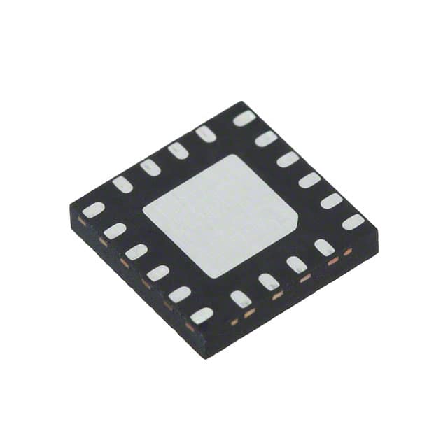
- Package: QFN (Quad Flat No-leads)
- Essence: Provides clock signals for various electronic systems
- Packaging/Quantity: Tape and Reel, 2500 units per reel
Specifications
- Frequency Range: 1 MHz to 808 MHz
- Output Type: LVCMOS, LVDS, HCSL
- Supply Voltage: 2.375V to 3.63V
- Operating Temperature Range: -40°C to +85°C
- Programmability: I2C Interface
Detailed Pin Configuration
The SI5335D-B03977-GM has a total of 20 pins. The pin configuration is as follows:
| Pin Number | Pin Name | Description | |------------|----------|-------------| | 1 | VDDO | Output Power Supply Voltage | | 2 | GND | Ground | | 3 | XAXB | Differential Clock Input | | 4 | XAXA | Differential Clock Input | | 5 | VDDI | Input Power Supply Voltage | | 6 | SDA | I2C Serial Data Input | | 7 | SCL | I2C Serial Clock Input | | 8 | GND | Ground | | 9 | CLKOUT0 | Clock Output | | 10 | CLKOUT1 | Clock Output | | 11 | CLKOUT2 | Clock Output | | 12 | CLKOUT3 | Clock Output | | 13 | CLKOUT4 | Clock Output | | 14 | CLKOUT5 | Clock Output | | 15 | CLKOUT6 | Clock Output | | 16 | CLKOUT7 | Clock Output | | 17 | GND | Ground | | 18 | VDDO | Output Power Supply Voltage | | 19 | VDDO | Output Power Supply Voltage | | 20 | GND | Ground |
Functional Features
- High-frequency clock generation and multiplication
- Low-jitter output signals for precise timing requirements
- Programmable frequency and output types
- I2C interface for easy configuration
- Wide operating temperature range for various environments
Advantages and Disadvantages
Advantages
- Provides a wide frequency range suitable for different applications
- Offers multiple output types to accommodate various systems
- Programmability allows flexibility in configuring clock signals
- Low-jitter output ensures accurate timing synchronization
Disadvantages
- Requires additional components for proper integration into a system
- Limited to a maximum frequency of 808 MHz
Working Principles
The SI5335D-B03977-GM is a clock generator and multiplier IC that generates high-frequency clock signals for electronic systems. It utilizes an internal PLL (Phase-Locked Loop) to multiply the input clock frequency and generate multiple output clocks with programmable frequencies and output types. The IC also incorporates a low-jitter design to ensure precise timing synchronization between different components within a system.
Detailed Application Field Plans
The SI5335D-B03977-GM finds applications in various fields where accurate and synchronized clock signals are required. Some of the potential application areas include: - Telecommunications equipment - Networking devices - Data centers - Industrial automation systems - Test and measurement instruments - Audio/video equipment
Detailed and Complete Alternative Models
- SI5338A-B-GM: Similar clock generator and multiplier IC with extended frequency range up to 1.4 GHz.
- SI5345A-B-GM: Clock generator and jitter attenuator IC with additional features for reducing clock signal noise.
- SI5368A-B-GM: Multi-channel clock generator IC with independent output dividers for precise synchronization in multi-board systems.
(Note: The above alternative models are provided for reference purposes and may have different specifications and pin configurations. Please refer to the respective datasheets for detailed information.)
Word count: 478 words
רשום 10 שאלות ותשובות נפוצות הקשורות ליישום של SI5335D-B03977-GM בפתרונות טכניים
Sure! Here are 10 common questions and answers related to the application of SI5335D-B03977-GM in technical solutions:
Q: What is the SI5335D-B03977-GM? A: The SI5335D-B03977-GM is a clock generator and jitter attenuator IC designed for use in various technical solutions.
Q: What are the key features of the SI5335D-B03977-GM? A: Some key features include multiple outputs, low jitter performance, programmable frequency synthesis, and flexible input/output configurations.
Q: How many outputs does the SI5335D-B03977-GM have? A: The SI5335D-B03977-GM has up to 12 differential outputs, which can be configured based on the specific requirements of the application.
Q: What is the purpose of a clock generator in a technical solution? A: A clock generator provides precise timing signals that synchronize various components within a system, ensuring proper operation and data integrity.
Q: Can the SI5335D-B03977-GM generate different frequencies for each output? A: Yes, the SI5335D-B03977-GM supports independent frequency programming for each output, allowing for versatile clocking configurations.
Q: How does the SI5335D-B03977-GM handle jitter attenuation? A: The SI5335D-B03977-GM utilizes advanced PLL-based techniques to reduce jitter, resulting in improved signal quality and reliability.
Q: What is the power supply voltage range for the SI5335D-B03977-GM? A: The SI5335D-B03977-GM operates from a single 3.3V power supply, making it compatible with standard power sources.
Q: Can the SI5335D-B03977-GM be programmed and configured? A: Yes, the SI5335D-B03977-GM can be programmed using an I2C interface, allowing for easy customization of its operating parameters.
Q: Is the SI5335D-B03977-GM suitable for high-speed data communication applications? A: Yes, the SI5335D-B03977-GM is designed to support high-speed data rates, making it suitable for applications such as Ethernet or PCIe.
Q: Are evaluation boards or reference designs available for the SI5335D-B03977-GM? A: Yes, Silicon Labs provides evaluation boards and reference designs that help developers quickly integrate the SI5335D-B03977-GM into their systems.
Please note that these answers are general and may vary depending on the specific requirements and application of the SI5335D-B03977-GM in a technical solution.