

NLAS4717MR2G
Product Overview
- Category: Integrated Circuit
- Use: Analog Switch
- Characteristics: High-speed, Low-power, Single-pole Double-throw (SPDT) switch
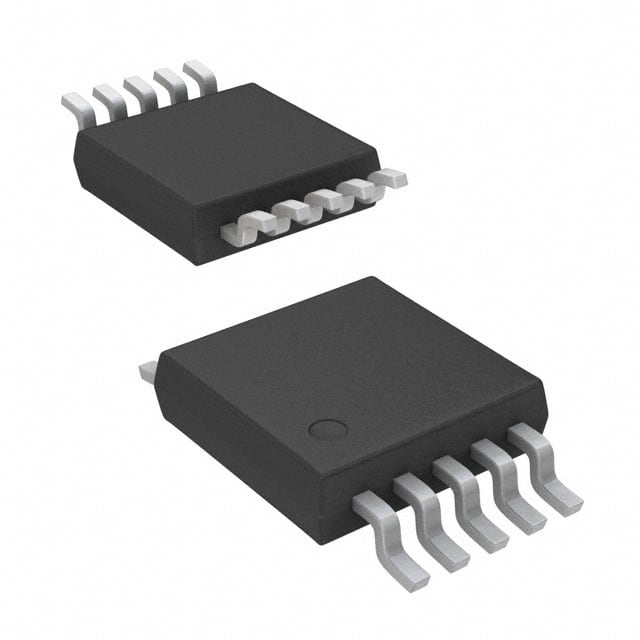
- Package: SOT-23-6
- Essence: Efficient signal routing and switching
- Packaging/Quantity: Tape and Reel, 3000 units per reel
Specifications
- Supply Voltage: 1.65V to 5.5V
- On-Resistance: 0.4Ω (typical)
- Off-Channel Leakage Current: 1nA (maximum)
- Switching Time: 20ns (typical)
- Operating Temperature Range: -40°C to +85°C
Detailed Pin Configuration
The NLAS4717MR2G has a total of 6 pins arranged as follows:
``` ___________ | | 1 | | 6 |___________|
2 | | 5
|___________|
3 | | 4
|___________|
```
Pin Description: 1. IN1: Input control for switch position 1 2. IN2: Input control for switch position 2 3. COM: Common terminal for both switch positions 4. NO: Normally Open contact 5. NC: Normally Closed contact 6. GND: Ground reference
Functional Features
- High-speed switching capability allows for efficient signal routing.
- Low power consumption makes it suitable for battery-powered devices.
- Single-pole double-throw (SPDT) configuration provides flexibility in signal routing.
Advantages and Disadvantages
Advantages: - Fast switching time enables quick signal routing. - Low on-resistance minimizes signal attenuation. - Wide operating voltage range allows for compatibility with various systems.
Disadvantages: - Limited number of switch positions (SPDT configuration). - Relatively small package size may require careful handling during assembly.
Working Principles
The NLAS4717MR2G is an analog switch that operates based on the control signals applied to the IN1 and IN2 pins. When a logic high signal is applied to IN1, the switch connects the COM terminal to the NO contact. Conversely, when a logic high signal is applied to IN2, the switch connects the COM terminal to the NC contact. The switch position is determined by the logical state of the control inputs.
Detailed Application Field Plans
The NLAS4717MR2G can be used in various applications, including but not limited to:
- Audio Systems: Signal routing in audio mixers, amplifiers, and effects processors.
- Communication Devices: Switching between different antennas or transmission lines.
- Test and Measurement Equipment: Signal switching for accurate measurements.
- Industrial Control Systems: Routing control signals in automation and process control.
Detailed and Complete Alternative Models
- NLAS4717MR2G is part of the NLAS series from ON Semiconductor, which includes other similar analog switches such as NLAS4684MR2G and NLAS4599MR2G.
- Analog Devices offers alternative models like ADG1419BRMZ and ADG1606BRUZ.
- Texas Instruments provides alternatives such as TS5A23157DGSR and TS3A24159DGSR.
These alternative models offer similar functionality and can be considered based on specific application requirements.
Word count: 408 words
רשום 10 שאלות ותשובות נפוצות הקשורות ליישום של NLAS4717MR2G בפתרונות טכניים
Sure! Here are 10 common questions and answers related to the application of NLAS4717MR2G in technical solutions:
Q: What is NLAS4717MR2G? A: NLAS4717MR2G is a specific model of a high-speed, low-power dual SPDT analog switch.
Q: What are the key features of NLAS4717MR2G? A: The key features of NLAS4717MR2G include low on-resistance, wide voltage range, low power consumption, and high bandwidth.
Q: What are the typical applications of NLAS4717MR2G? A: NLAS4717MR2G is commonly used in various technical solutions such as audio and video signal routing, data acquisition systems, communication devices, and battery-powered portable devices.
Q: What is the voltage range supported by NLAS4717MR2G? A: NLAS4717MR2G supports a wide voltage range from -5V to +5V, making it suitable for both single-supply and dual-supply applications.
Q: How does NLAS4717MR2G achieve low power consumption? A: NLAS4717MR2G utilizes advanced CMOS technology, which enables it to operate at low power levels while maintaining high performance.
Q: Can NLAS4717MR2G handle high-frequency signals? A: Yes, NLAS4717MR2G has a high bandwidth capability, allowing it to handle high-frequency signals up to several hundred megahertz.
Q: Is NLAS4717MR2G compatible with digital logic levels? A: Yes, NLAS4717MR2G is designed to be compatible with standard digital logic levels, making it easy to interface with microcontrollers and other digital devices.
Q: Can NLAS4717MR2G be used in battery-powered devices? A: Yes, NLAS4717MR2G is designed for low power consumption, making it suitable for use in battery-powered devices where energy efficiency is crucial.
Q: Does NLAS4717MR2G have built-in protection features? A: Yes, NLAS4717MR2G incorporates built-in ESD protection, ensuring robustness against electrostatic discharge events.
Q: Are there any recommended alternatives to NLAS4717MR2G? A: While NLAS4717MR2G is a popular choice, alternative analog switches from different manufacturers, such as ADG721 or MAX4617, can also be considered based on specific requirements.
Please note that the answers provided here are general and may vary depending on the specific application and context.