

NCP1253BSN65T1G - English Editing Encyclopedia Entry
Product Overview
Category
The NCP1253BSN65T1G belongs to the category of integrated circuits (ICs) specifically designed for power management applications.
Use
This IC is commonly used in various electronic devices and systems to regulate and control power supply, ensuring efficient and reliable operation.
Characteristics
- The NCP1253BSN65T1G offers high efficiency power conversion, making it suitable for energy-conscious applications.
- It features a compact design, allowing for space-saving integration into electronic devices.
- This IC provides excellent voltage regulation and protection against overvoltage, overcurrent, and short circuits.
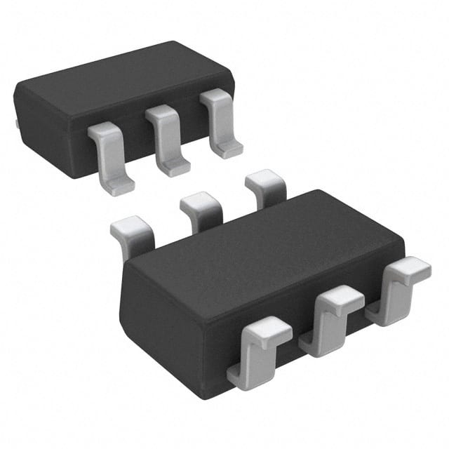
Package
The NCP1253BSN65T1G is available in a small outline package (SOP), which facilitates easy installation and soldering onto circuit boards.
Essence
The essence of this IC lies in its ability to efficiently manage power supply, ensuring stable and reliable operation of electronic devices.
Packaging/Quantity
The NCP1253BSN65T1G is typically packaged in reels, with each reel containing a specific quantity of ICs. The exact quantity may vary depending on the manufacturer's specifications.
Specifications
- Input Voltage Range: 85V to 265V AC
- Output Voltage Range: Adjustable, typically 5V to 24V DC
- Maximum Output Current: 2.5A
- Switching Frequency: 65kHz
- Operating Temperature Range: -40°C to +125°C
Detailed Pin Configuration
The NCP1253BSN65T1G has the following pin configuration:
- VCC: Power supply input
- GND: Ground reference
- FB: Feedback pin for output voltage regulation
- COMP: Compensation pin for stability control
- CS: Current sense pin for current regulation
- DRAIN: Switching transistor drain pin
- VCCSENSE: Voltage sensing pin for VCC regulation
Functional Features
- Integrated high-voltage startup circuitry for simplified power supply design.
- Pulse frequency modulation (PFM) control for improved efficiency at light loads.
- Built-in protection features such as overvoltage, overcurrent, and short circuit protection.
- Soft-start function to prevent excessive inrush current during startup.
Advantages and Disadvantages
Advantages
- High efficiency power conversion, reducing energy consumption.
- Compact design for space-saving integration.
- Excellent voltage regulation and protection features ensure device reliability.
Disadvantages
- Limited maximum output current of 2.5A may not be suitable for high-power applications.
- Operating temperature range may restrict usage in extreme environments.
Working Principles
The NCP1253BSN65T1G operates based on a pulse frequency modulation (PFM) control scheme. It regulates the output voltage by adjusting the switching frequency of the internal power switch. This allows for efficient power conversion across a wide input voltage range.
Detailed Application Field Plans
The NCP1253BSN65T1G finds application in various electronic devices and systems, including but not limited to: - Power adapters and chargers - LED lighting systems - Industrial automation equipment - Consumer electronics
Detailed and Complete Alternative Models
- NCP1253BDR2G
- NCP1253ADR2G
- NCP1253BDR2
- NCP1253ADR2
- NCP1253BPG
- NCP1253APG
These alternative models offer similar functionality and can be considered as substitutes for the NCP1253BSN65T1G depending on specific requirements.
Word count: 526 words
רשום 10 שאלות ותשובות נפוצות הקשורות ליישום של NCP1253BSN65T1G בפתרונות טכניים
Sure! Here are 10 common questions and answers related to the application of NCP1253BSN65T1G in technical solutions:
Q1: What is NCP1253BSN65T1G? A1: NCP1253BSN65T1G is a highly integrated PWM controller IC designed for offline flyback converters. It provides various features like high voltage startup, current mode control, and protection functions.
Q2: What is the input voltage range for NCP1253BSN65T1G? A2: The input voltage range for NCP1253BSN65T1G is typically between 85V and 265V AC.
Q3: What is the maximum output power that can be achieved with NCP1253BSN65T1G? A3: The maximum output power depends on the specific design and application, but NCP1253BSN65T1G can handle power levels up to several tens of watts.
Q4: Can NCP1253BSN65T1G be used in both isolated and non-isolated applications? A4: Yes, NCP1253BSN65T1G can be used in both isolated and non-isolated applications, making it versatile for various power supply designs.
Q5: Does NCP1253BSN65T1G have built-in protection features? A5: Yes, NCP1253BSN65T1G includes various protection features such as overvoltage protection (OVP), overload protection (OLP), and thermal shutdown.
Q6: What is the switching frequency range of NCP1253BSN65T1G? A6: The switching frequency range of NCP1253BSN65T1G is typically between 20kHz and 100kHz, but it can be adjusted using external components.
Q7: Can NCP1253BSN65T1G operate in a wide temperature range? A7: Yes, NCP1253BSN65T1G is designed to operate in a wide temperature range, typically from -40°C to 125°C.
Q8: What type of feedback control does NCP1253BSN65T1G support? A8: NCP1253BSN65T1G supports voltage mode control, which is commonly used in flyback converter applications.
Q9: Is NCP1253BSN65T1G suitable for low standby power applications? A9: Yes, NCP1253BSN65T1G has a low standby power consumption and can be used in designs that require low power in standby mode.
Q10: Are there any evaluation boards or reference designs available for NCP1253BSN65T1G? A10: Yes, ON Semiconductor provides evaluation boards and reference designs for NCP1253BSN65T1G, which can help in the development and testing of power supply solutions.
Please note that these answers are general and may vary depending on specific design requirements and application scenarios.