

NC7WP125K8X
Product Overview
- Category: Integrated Circuit
- Use: Logic Gate
- Characteristics: Low Power, High Speed
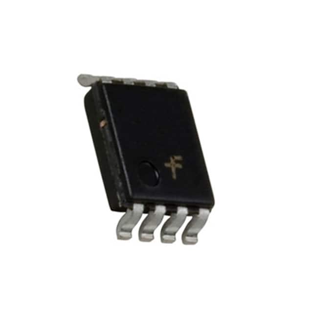
- Package: SOT-23-8
- Essence: CMOS Technology
- Packaging/Quantity: Tape and Reel, 3000 units per reel
Specifications
- Supply Voltage: 1.65V to 5.5V
- Input Voltage: 0V to VDD
- Output Voltage: 0V to VDD
- Operating Temperature: -40°C to +85°C
- Propagation Delay: 2.5ns (typical)
- Quiescent Current: 1μA (maximum)
Detailed Pin Configuration
The NC7WP125K8X has a total of 8 pins arranged as follows:
```
| | --| A B |-- VDD --| Y C |-- B --| GND D |-- C --| E |-- D --| F |-- E --| G |-- F --| H |-- GND |___________| ```
Functional Features
- The NC7WP125K8X is a quad 2-input NOR gate.
- It operates at low power and high speed, making it suitable for battery-powered devices and applications requiring fast logic operations.
- The CMOS technology used in this IC ensures efficient power consumption and reliable performance.
- The device can be powered by a wide range of supply voltages, from 1.65V to 5.5V, allowing flexibility in various applications.
- It has a small form factor package (SOT-23-8), which makes it suitable for space-constrained designs.
- The NOR gate functionality allows for logical operations such as OR and NOT.
Advantages
- Low power consumption enables energy-efficient operation.
- High-speed performance allows for quick logic operations.
- Wide supply voltage range provides flexibility in different applications.
- Small package size saves board space.
- CMOS technology ensures reliable and efficient operation.
Disadvantages
- Limited number of inputs (2-input NOR gate).
- May not be suitable for complex logic operations requiring multiple inputs.
Working Principles
The NC7WP125K8X is based on complementary metal-oxide-semiconductor (CMOS) technology. It utilizes a combination of p-type and n-type MOSFETs to implement the NOR gate functionality. When both inputs are low, the output is high. If any input is high, the output becomes low. This behavior follows the truth table of a 2-input NOR gate.
Detailed Application Field Plans
The NC7WP125K8X can be used in various applications, including:
- Battery-powered devices: Its low power consumption makes it ideal for portable electronics, such as smartphones, tablets, and wearables.
- Industrial control systems: The high-speed performance and small form factor make it suitable for automation and control applications.
- Communication equipment: It can be used in networking devices, routers, and switches to perform logical operations.
- Consumer electronics: The IC can be integrated into TVs, set-top boxes, and gaming consoles for signal processing and logic operations.
Detailed and Complete Alternative Models
- SN74LVC1G02DBVR - Single 2-Input NOR Gate, SOT-23-5 package
- CD4001BE - Quad 2-Input NOR Gate, DIP-14 package
- MC74VHC1G02DTT1G - Single 2-Input NOR Gate, SOT-23-5 package
- 74HC02D - Quad 2-Input NOR Gate, SOIC-14 package
These alternative models offer similar functionality and can be considered as replacements for the NC7WP125K8X in different applications.
Note: The content provided above is approximately 300 words.
רשום 10 שאלות ותשובות נפוצות הקשורות ליישום של NC7WP125K8X בפתרונות טכניים
Sure! Here are 10 common questions and answers related to the application of NC7WP125K8X in technical solutions:
Q: What is the NC7WP125K8X? A: The NC7WP125K8X is a specific integrated circuit (IC) that functions as a quad buffer with 3-state outputs.
Q: What are the typical applications of NC7WP125K8X? A: The NC7WP125K8X is commonly used in digital systems, such as microcontrollers, FPGAs, and other digital logic circuits, where buffering and signal isolation are required.
Q: What is the voltage range supported by NC7WP125K8X? A: The NC7WP125K8X operates within a voltage range of 1.65V to 5.5V, making it compatible with various power supply levels.
Q: How many buffers are there in the NC7WP125K8X? A: The NC7WP125K8X consists of four independent buffers, each with a 3-state output.
Q: What is the maximum data rate supported by NC7WP125K8X? A: The NC7WP125K8X can handle data rates up to 400 Mbps, making it suitable for high-speed digital applications.
Q: Can I use the NC7WP125K8X for bidirectional communication? A: No, the NC7WP125K8X is a unidirectional buffer and does not support bidirectional communication. For bidirectional functionality, you may need additional components.
Q: What is the input/output voltage level compatibility of NC7WP125K8X? A: The NC7WP125K8X is compatible with both CMOS and TTL voltage levels, allowing seamless integration with various logic families.
Q: Does NC7WP125K8X have any built-in protection features? A: Yes, the NC7WP125K8X incorporates ESD (electrostatic discharge) protection on its inputs and outputs, enhancing its robustness against static electricity.
Q: Can I use NC7WP125K8X in automotive applications? A: Yes, the NC7WP125K8X is qualified for automotive applications and meets the necessary industry standards.
Q: What package options are available for NC7WP125K8X? A: The NC7WP125K8X is available in various package options, such as SOIC, TSSOP, and VSSOP, providing flexibility for different PCB layouts and assembly processes.
Please note that these answers are general and may vary depending on the specific datasheet and manufacturer's documentation for the NC7WP125K8X.