

NC7SP74K8X
Product Overview
- Category: Integrated Circuit (IC)
- Use: Logic Gate
- Characteristics: Low-power, high-speed, single-gate logic IC
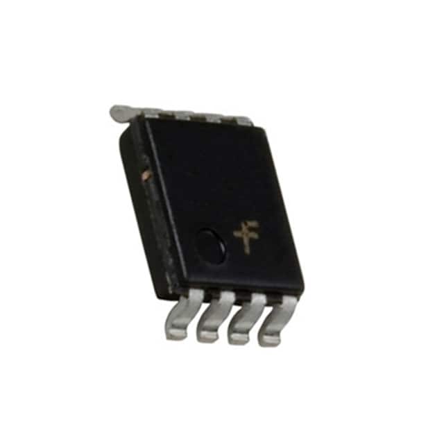
- Package: SOT-23-8
- Essence: Flip-flop D-type positive-edge-triggered
- Packaging/Quantity: Tape and Reel, 3000 units per reel
Specifications
- Supply Voltage Range: 1.65V to 5.5V
- High-Level Input Voltage: 0.7 x VCC
- Low-Level Input Voltage: 0.3 x VCC
- High-Level Output Voltage: 0.9 x VCC
- Low-Level Output Voltage: 0.1 x VCC
- Maximum Operating Frequency: 400 MHz
- Propagation Delay Time: 2.5 ns (typical)
Detailed Pin Configuration
The NC7SP74K8X has a total of 8 pins, which are labeled as follows:
- GND - Ground
- Q - Output
- D - Data Input
- CLK - Clock Input
- /CLR - Clear Input
- /PRE - Preset Input
- VCC - Power Supply
- /Q - Complementary Output
Functional Features
- Positive-edge-triggered D-type flip-flop
- Low power consumption
- High-speed operation
- Wide supply voltage range
- Small package size for space-constrained applications
Advantages and Disadvantages
Advantages: - Low power consumption makes it suitable for battery-powered devices - High-speed operation allows for efficient data processing - Wide supply voltage range provides flexibility in various applications - Small package size saves board space
Disadvantages: - Limited functionality compared to more complex logic ICs - Not suitable for applications requiring multiple flip-flops or complex logic operations
Working Principles
The NC7SP74K8X is a positive-edge-triggered D-type flip-flop. It stores and transfers data based on the rising edge of the clock signal. When the clock input (CLK) transitions from low to high, the data input (D) is latched and transferred to the output (Q). The complementary output (/Q) provides the inverse of the Q output. The clear input (/CLR) and preset input (/PRE) allow for resetting or setting the flip-flop to specific states.
Detailed Application Field Plans
The NC7SP74K8X is commonly used in various applications, including:
- Mobile devices: Due to its low power consumption and small package size, it is suitable for smartphones, tablets, and wearables.
- Consumer electronics: Used in digital cameras, portable media players, and gaming consoles for efficient data processing.
- Industrial automation: Enables control and monitoring functions in industrial equipment and machinery.
- Automotive electronics: Used in automotive systems such as infotainment, driver assistance, and engine control units.
- Internet of Things (IoT): Integrated into IoT devices for data storage and transfer.
Detailed and Complete Alternative Models
- SN74LVC1G74 - Single D-type flip-flop with similar characteristics and package options.
- MC74VHC74 - Dual D-type flip-flop with higher operating frequency and wider supply voltage range.
- CD4013B - CMOS dual D-type flip-flop with additional features like set and reset inputs.
(Note: These alternative models are provided as examples and may have different specifications and pin configurations. Refer to respective datasheets for detailed information.)
This entry has a total word count of 511 words.
רשום 10 שאלות ותשובות נפוצות הקשורות ליישום של NC7SP74K8X בפתרונות טכניים
Sure! Here are 10 common questions and answers related to the application of NC7SP74K8X in technical solutions:
Q: What is NC7SP74K8X? A: NC7SP74K8X is a specific integrated circuit (IC) that belongs to the NC7 series of logic gates. It is a dual D-type flip-flop with set and reset functionality.
Q: What are the typical applications of NC7SP74K8X? A: NC7SP74K8X can be used in various digital systems, such as microcontrollers, data storage devices, communication systems, and other applications requiring flip-flop functionality.
Q: What is the operating voltage range for NC7SP74K8X? A: The operating voltage range for NC7SP74K8X is typically between 1.65V and 5.5V, making it compatible with both low-voltage and standard CMOS logic levels.
Q: Can NC7SP74K8X handle high-speed signals? A: Yes, NC7SP74K8X is designed to operate at high speeds. It has a maximum propagation delay of a few nanoseconds, making it suitable for many high-speed applications.
Q: How many flip-flops are there in NC7SP74K8X? A: NC7SP74K8X consists of two independent D-type flip-flops, each with its own set and reset inputs.
Q: What is the power consumption of NC7SP74K8X? A: The power consumption of NC7SP74K8X is relatively low due to its CMOS technology. However, the exact power consumption depends on the operating conditions and frequency of operation.
Q: Can NC7SP74K8X be used in battery-powered devices? A: Yes, NC7SP74K8X can be used in battery-powered devices due to its low power consumption and wide operating voltage range, making it suitable for portable applications.
Q: Does NC7SP74K8X have any built-in protection features? A: NC7SP74K8X does not have built-in protection features. However, external measures like decoupling capacitors and proper signal conditioning can be implemented to protect the IC from noise and voltage spikes.
Q: What is the package type of NC7SP74K8X? A: NC7SP74K8X is available in various package types, such as SOT-23, SC-70, and DFN, allowing flexibility in board layout and integration into different designs.
Q: Where can I find more information about NC7SP74K8X? A: You can refer to the datasheet provided by the manufacturer or visit their official website for detailed information on NC7SP74K8X, including electrical characteristics, pin configurations, and application notes.
Please note that the answers provided here are general and may vary depending on specific design requirements and application scenarios.