

NB7L1008MMNTWG
Overview
- Category: Integrated Circuit (IC)
- Use: Signal Distribution and Clock Generation
- Characteristics: High-speed, Low-power, Differential Input/Output
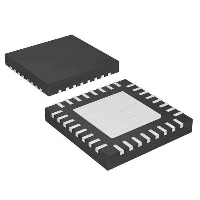
- Package: 48-pin QFN (Quad Flat No-Lead)
- Essence: Clock Divider and Multiplexer
- Packaging/Quantity: Tape and Reel, 2500 units per reel
Specifications and Parameters
- Supply Voltage: 2.375V to 3.465V
- Input Frequency Range: DC to 10GHz
- Output Frequency Range: DC to 10GHz
- Input Signal Types: Differential or Single-ended
- Output Signal Types: Differential
- Number of Inputs: 1
- Number of Outputs: 8
- Operating Temperature Range: -40°C to +85°C
Pin Configuration
The NB7L1008MMNTWG has a total of 48 pins. The pin configuration is as follows:
| Pin Number | Pin Name | Description | |------------|----------|-------------| | 1 | VCC | Power Supply Voltage | | 2 | GND | Ground | | 3 | INP | Positive Differential Input | | 4 | INN | Negative Differential Input | | 5-12 | OUT0-OUT7 | Differential Outputs | | 13 | SEL | Select Input | | 14-17 | NC | No Connection | | 18 | VREF | Reference Voltage | | 19-22 | NC | No Connection | | 23 | OE | Output Enable | | 24-48 | NC | No Connection |
Functional Characteristics
- The NB7L1008MMNTWG is a clock divider and multiplexer IC.
- It accepts a single-ended or differential input signal and generates eight differential output signals.
- The output frequency can be divided by 1, 2, 4, or 8, depending on the select input.
- The IC operates at high speeds up to 10GHz and consumes low power.
- It has an output enable pin for easy control of the output signals.
Advantages and Disadvantages
Advantages: - High-speed operation - Low power consumption - Differential input and output - Output enable feature for easy control
Disadvantages: - Limited number of inputs (only one) - Limited output frequency division options (1, 2, 4, or 8)
Applicable Range of Products
The NB7L1008MMNTWG is suitable for applications that require signal distribution and clock generation. It can be used in various electronic systems, including communication devices, data centers, and high-speed digital designs.
Working Principles
The IC operates by accepting a single-ended or differential input signal through the INP and INN pins. The input signal is then divided and multiplexed based on the select input (SEL). The resulting eight differential output signals (OUT0-OUT7) have frequencies that are divided by 1, 2, 4, or 8, depending on the select input.
Detailed Application Field Plans
The NB7L1008MMNTWG can be used in the following application fields: 1. Communication Systems: Signal distribution and clock generation in wireless communication devices, such as base stations and routers. 2. Data Centers: Clock synchronization and signal distribution in high-speed data processing systems. 3. Test and Measurement Equipment: Signal routing and distribution in oscilloscopes, logic analyzers, and other test instruments. 4. Networking Equipment: Clock generation and distribution in switches, routers, and network interface cards. 5. High-Speed Digital Designs: Signal distribution and clock generation in FPGA (Field-Programmable Gate Array) and ASIC (Application-Specific Integrated Circuit) designs.
Detailed Alternative Models
Some alternative models to the NB7L1008MMNTWG are: 1. NB7L1008R: Similar functionality, but with a different package (48-pin BGA). 2. MC1008: Comparable clock divider and multiplexer IC from a different manufacturer. 3. CDCLVC1108: Clock divider and multiplexer IC with similar features and pin configuration. 4. SY100EP11: Differential clock divider and multiplexer IC with additional features for ECL (Emitter-Coupled Logic) compatibility. 5. MAX999: High-speed clock divider and multiplexer IC with adjustable output frequency division ratios.
5 Common Technical Questions and Answers
Q: What is the maximum input frequency supported by the NB7L1008MMNTWG? A: The IC can accept input frequencies up to 10GHz.
Q: Can I use a single-ended input signal with this IC? A: Yes, the NB7L1008