

Encyclopedia Entry: 74ABT374CMTC
Product Overview
Category
The 74ABT374CMTC belongs to the category of integrated circuits (ICs) and specifically falls under the family of flip-flops.
Use
This IC is commonly used in digital electronics for storing and transferring data. It is primarily employed in applications where sequential logic is required, such as in microprocessors, memory systems, and communication devices.
Characteristics
- High-speed operation: The 74ABT374CMTC offers fast data transfer rates, making it suitable for time-critical applications.
- Low power consumption: This IC is designed to minimize power consumption, ensuring efficient operation.
- Wide voltage range: It can operate within a wide voltage range, typically between 2V and 5.5V.
- Schmitt-trigger inputs: The IC incorporates Schmitt-trigger inputs, which provide hysteresis and improve noise immunity.
Package and Quantity
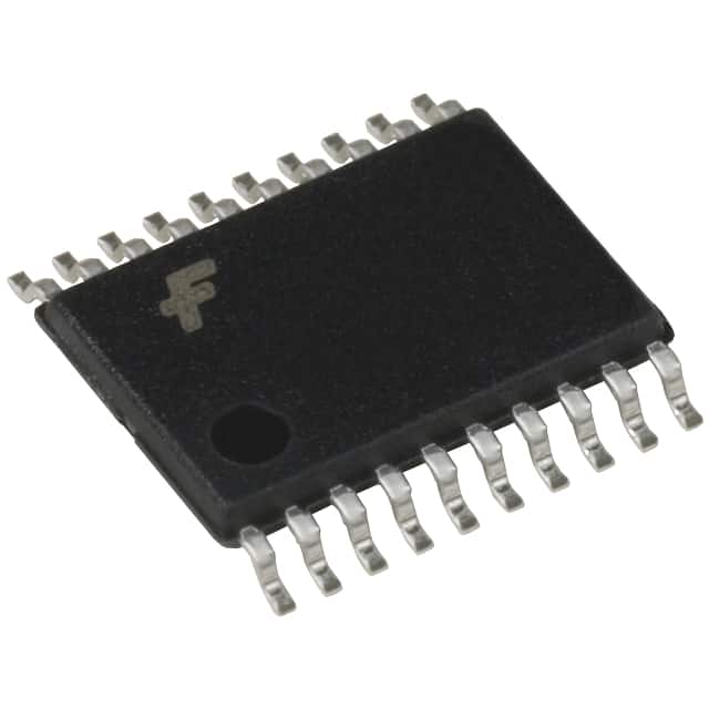
The 74ABT374CMTC is available in a small outline integrated circuit (SOIC) package. It consists of 20 pins and is supplied in tape and reel packaging. Each reel typically contains 250 units.
Specifications
- Supply Voltage Range: 2V to 5.5V
- Input Voltage Range: 0V to VCC
- Output Voltage Range: 0V to VCC
- Operating Temperature Range: -40°C to +85°C
- Maximum Clock Frequency: 100 MHz
- Propagation Delay: 3.5 ns (typical)
Pin Configuration
The pin configuration of the 74ABT374CMTC is as follows:
+---+--+---+
   D0 -|1  +--+ 20|- VCC
   D1 -|2         |- D7
   D2 -|3         |- OE
   D3 -|4         |- CP
   D4 -|5         |- Q7
   D5 -|6         |- Q6
   D6 -|7         |- Q5
  GND -|8         |- Q4
   Q0 -|9         |- Q3
   Q1 -|10        |- Q2
       +----------+
Functional Features
The 74ABT374CMTC is a positive-edge triggered octal D-type flip-flop with three-state outputs. It can store and transfer data on the rising edge of the clock signal (CP). The output enable (OE) pin allows for tri-state operation, enabling multiple devices to share a common bus.
Advantages and Disadvantages
Advantages
- High-speed operation enables efficient data transfer.
- Low power consumption ensures energy efficiency.
- Wide voltage range allows for compatibility with various systems.
- Schmitt-trigger inputs enhance noise immunity.
Disadvantages
- Limited number of flip-flops in a single IC package.
- May require additional components for complex applications.
Working Principles
The 74ABT374CMTC operates based on the principles of sequential logic. When the clock signal (CP) transitions from low to high (rising edge), the input data (D0-D7) is latched and stored in the flip-flops. The stored data is then available at the corresponding output pins (Q0-Q7). The output enable (OE) pin controls whether the outputs are active or in a high-impedance state.
Application Field Plans
The 74ABT374CMTC finds extensive use in various digital systems, including but not limited to: - Microprocessors and microcontrollers - Memory systems (RAM, ROM) - Communication devices (routers, switches) - Data storage systems - Industrial automation equipment
Alternative Models
Several alternative models with similar functionality are available in the market. Some notable alternatives to the 74ABT374CMTC include: - 74HC374: A CMOS-based octal D-type flip-flop with three-state outputs. - SN74LS374: A TTL-based octal D-type flip-flop with tri-state outputs. - CD4013: A dual D-type flip-flop with complementary outputs.
These alternative models can be considered based on specific application requirements and compatibility with existing systems.
In conclusion, the 74ABT374CMTC is a high-speed, low-power octal D-type flip-flop IC used for sequential logic applications. Its wide voltage range, Schmitt-trigger inputs, and three-state outputs make it suitable for various digital systems. While it has certain limitations, there are alternative models available to cater to different needs within the same functional category.
רשום 10 שאלות ותשובות נפוצות הקשורות ליישום של 74ABT374CMTC בפתרונות טכניים
Sure! Here are 10 common questions and answers related to the application of 74ABT374CMTC in technical solutions:
Q: What is the 74ABT374CMTC? A: The 74ABT374CMTC is a type of integrated circuit (IC) that functions as an octal D-type flip-flop with 3-state outputs.
Q: What is the purpose of using the 74ABT374CMTC in technical solutions? A: The 74ABT374CMTC is commonly used for data storage, synchronization, and signal buffering in digital systems.
Q: How many flip-flops are there in the 74ABT374CMTC? A: The 74ABT374CMTC consists of eight individual D-type flip-flops.
Q: What is the significance of the 3-state outputs in the 74ABT374CMTC? A: The 3-state outputs allow the IC to be connected to a bus or shared line without interfering with other devices on the same line.
Q: What is the maximum operating frequency of the 74ABT374CMTC? A: The maximum operating frequency of the 74ABT374CMTC is typically specified by the manufacturer and can vary, but it is commonly in the range of several hundred megahertz.
Q: Can the 74ABT374CMTC be used in both synchronous and asynchronous applications? A: Yes, the 74ABT374CMTC can be used in both synchronous and asynchronous applications depending on the specific requirements of the system.
Q: What is the power supply voltage range for the 74ABT374CMTC? A: The typical power supply voltage range for the 74ABT374CMTC is between 4.5V and 5.5V.
Q: How does the 74ABT374CMTC handle input data during the setup time? A: The 74ABT374CMTC latches the input data during the setup time and holds it until the next clock edge.
Q: Can the 74ABT374CMTC be cascaded to increase the number of flip-flops? A: Yes, multiple 74ABT374CMTC ICs can be cascaded together to increase the number of flip-flops in a system.
Q: Are there any specific precautions to consider when using the 74ABT374CMTC? A: It is important to ensure proper decoupling capacitors are used near the power supply pins and to follow the manufacturer's guidelines for layout and thermal considerations to ensure reliable operation.