

PZM3.0NB2,115
Introduction
PZM3.0NB2,115 is a semiconductor product that belongs to the category of diodes. This entry provides an overview of its basic information, specifications, detailed pin configuration, functional features, advantages and disadvantages, working principles, detailed application field plans, and alternative models.
Basic Information Overview
- Category: Diodes
- Use: Rectification and signal demodulation in electronic circuits
- Characteristics: Small form factor, high reliability, low forward voltage drop
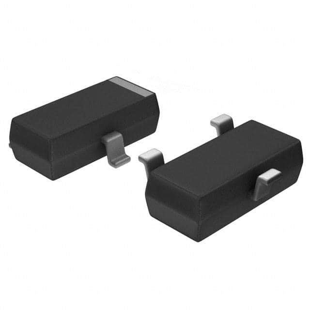
- Package: SOD-123FL
- Essence: High-speed switching diode
- Packaging/Quantity: Tape and reel, 3000 units per reel
Specifications
- Forward Voltage: 1V
- Reverse Voltage: 75V
- Forward Current: 200mA
- Reverse Recovery Time: 4ns
- Operating Temperature Range: -55°C to +150°C
Detailed Pin Configuration
The PZM3.0NB2,115 has two pins: 1. Anode (A) 2. Cathode (K)
Functional Features
- Fast switching speed
- Low leakage current
- High surge current capability
- Miniature SOD-123FL package for space-constrained applications
Advantages and Disadvantages
Advantages
- High-speed performance
- Compact package size
- Low forward voltage drop
Disadvantages
- Limited reverse voltage rating
- Sensitivity to overvoltage conditions
Working Principles
The PZM3.0NB2,115 operates based on the principles of semiconductor physics, utilizing its PN junction to allow current flow in one direction while blocking it in the reverse direction.
Detailed Application Field Plans
The PZM3.0NB2,115 is suitable for various applications, including: - High-frequency rectification in RF circuits - Signal demodulation in communication systems - Switching and clamping circuits in electronic equipment
Detailed and Complete Alternative Models
- 1N4148: General-purpose switching diode
- BAV99: Dual common cathode switching diode
- BAT54S: Schottky barrier diode
In conclusion, the PZM3.0NB2,115 is a high-speed switching diode with a compact form factor, making it suitable for various electronic applications requiring fast signal processing and rectification.
Word count: 322
רשום 10 שאלות ותשובות נפוצות הקשורות ליישום של PZM3.0NB2,115 בפתרונות טכניים
What is PZM3.0NB2,115?
- PZM3.0NB2,115 is a specific type of semiconductor diode used in various technical solutions.
What are the key features of PZM3.0NB2,115?
- PZM3.0NB2,115 features include a low forward voltage drop, high current capability, and fast switching speed.
In what technical applications can PZM3.0NB2,115 be used?
- PZM3.0NB2,115 can be used in voltage regulation, signal processing, power management, and protection circuits.
What is the maximum current rating for PZM3.0NB2,115?
- The maximum current rating for PZM3.0NB2,115 is typically around 200mA.
What is the typical forward voltage drop of PZM3.0NB2,115?
- The typical forward voltage drop of PZM3.0NB2,115 is around 0.7V at a specified current.
How does PZM3.0NB2,115 compare to other diodes in terms of performance?
- PZM3.0NB2,115 offers lower forward voltage drop and higher current capability compared to standard silicon diodes.
Can PZM3.0NB2,115 be used in high-frequency applications?
- Yes, PZM3.0NB2,115's fast switching speed makes it suitable for high-frequency applications such as RF circuits.
What are the temperature limitations for PZM3.0NB2,115?
- PZM3.0NB2,115 typically has a temperature range from -55°C to 150°C, making it suitable for a wide range of operating conditions.
Are there any specific layout considerations when using PZM3.0NB2,115 in a circuit?
- It is important to minimize the length of the traces connected to PZM3.0NB2,115 to reduce parasitic inductance and maintain signal integrity.
Where can I find detailed specifications and application notes for PZM3.0NB2,115?
- Detailed specifications and application notes for PZM3.0NB2,115 can be found in the manufacturer's datasheet and technical documentation.