

PZM20NB2,115
Introduction
PZM20NB2,115 is a semiconductor product belonging to the category of Zener diodes. This entry provides an overview of its basic information, specifications, pin configuration, functional features, advantages and disadvantages, working principles, application field plans, and alternative models.
Basic Information Overview
- Category: Zener Diode
- Use: Voltage regulation and protection in electronic circuits
- Characteristics: Precise voltage regulation, low impedance, and high reliability
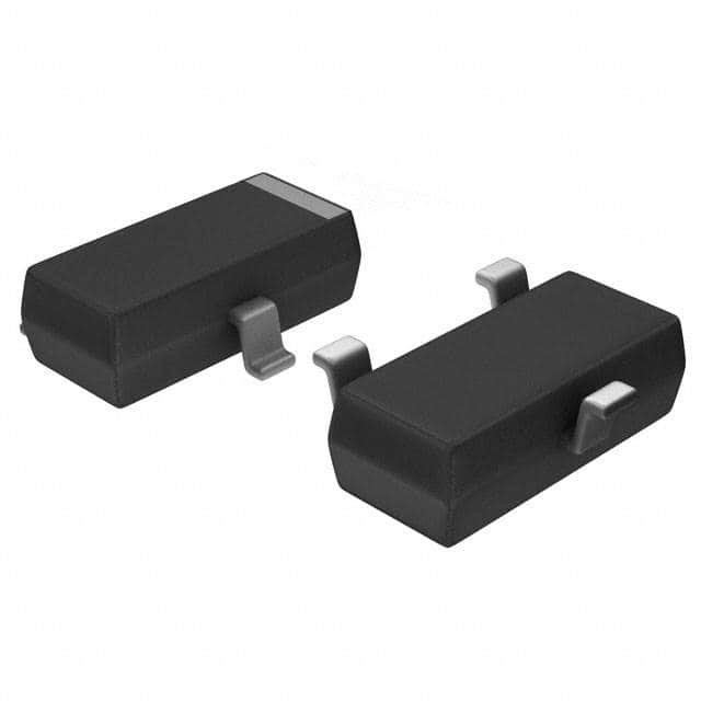
- Package: SOD123FL
- Essence: Semiconductor material with specific doping to achieve desired voltage characteristics
- Packaging/Quantity: Tape and Reel, 3000 units per reel
Specifications
- Voltage: 20V
- Power Dissipation: 225mW
- Zener Impedance: 40Ω
- Operating Temperature Range: -65°C to +150°C
- Storage Temperature Range: -65°C to +175°C
Detailed Pin Configuration
The PZM20NB2,115 Zener diode has a standard SOD123FL package with two pins. The pinout configuration is as follows: 1. Anode (A) 2. Cathode (K)
Functional Features
- Precise Voltage Regulation: Maintains a constant voltage across the diode under varying load conditions.
- Overvoltage Protection: Safeguards sensitive components in electronic circuits by diverting excess voltage.
- Low Impedance: Allows for efficient current flow while regulating voltage.
Advantages and Disadvantages
Advantages
- Reliable voltage regulation
- Compact SOD123FL package
- Low impedance for efficient operation
Disadvantages
- Limited power dissipation capability
- Narrow operating temperature range
Working Principles
The PZM20NB2,115 operates based on the principle of the Zener effect, where it maintains a constant voltage drop across its terminals when reverse-biased. This allows it to regulate voltage in electronic circuits and protect against overvoltage conditions.
Detailed Application Field Plans
The PZM20NB2,115 Zener diode finds applications in various electronic circuits, including: - Voltage regulators in power supplies - Overvoltage protection in communication equipment - Signal clamping and limiting circuits
Detailed and Complete Alternative Models
- PZM3NB2,115: 3V Zener diode with similar characteristics
- PZM5NB2,115: 5V Zener diode suitable for low-voltage applications
- PZM15NB2,115: 15V Zener diode offering higher voltage regulation
In conclusion, the PZM20NB2,115 Zener diode offers precise voltage regulation and overvoltage protection in a compact package, making it suitable for various electronic applications.
Word Count: 366
רשום 10 שאלות ותשובות נפוצות הקשורות ליישום של PZM20NB2,115 בפתרונות טכניים
What is the operating temperature range of PZM20NB2,115?
- The operating temperature range of PZM20NB2,115 is typically -55°C to +150°C.
What is the maximum power dissipation of PZM20NB2,115?
- The maximum power dissipation of PZM20NB2,115 is 500 mW.
What is the breakdown voltage of PZM20NB2,115?
- The breakdown voltage of PZM20NB2,115 is typically 20 V.
What is the capacitance range of PZM20NB2,115?
- The capacitance range of PZM20NB2,115 is typically 2.5 pF to 12 pF.
What are the typical applications for PZM20NB2,115?
- PZM20NB2,115 is commonly used in voltage regulation, signal clamping, and voltage reference circuits.
What is the package type of PZM20NB2,115?
- PZM20NB2,115 is available in a SOD-323 package.
What is the reverse leakage current of PZM20NB2,115?
- The reverse leakage current of PZM20NB2,115 is typically 0.1 µA.
What are the key features of PZM20NB2,115?
- PZM20NB2,115 features low leakage current, high stability, and fast response time.
What are the recommended storage conditions for PZM20NB2,115?
- It is recommended to store PZM20NB2,115 in a dry and cool environment, preferably with a temperature range of -55°C to +150°C.
What are the soldering recommendations for PZM20NB2,115?
- When soldering PZM20NB2,115, it is advised to use a soldering iron with a temperature of 260°C for no more than 10 seconds to prevent damage to the component.