

Encyclopedia Entry: 74VHC595BQ,115
Product Overview
Category
The 74VHC595BQ,115 belongs to the category of integrated circuits (ICs) and specifically falls under the family of shift registers.
Use
This IC is commonly used for serial-in, parallel-out (SIPO) data shifting applications. It allows for efficient control of multiple outputs using a minimal number of pins on a microcontroller or other digital devices.
Characteristics
- High-speed operation: The 74VHC595BQ,115 operates at high clock frequencies, making it suitable for time-critical applications.
- Low power consumption: This IC is designed to minimize power consumption, making it ideal for battery-powered devices.
- Wide operating voltage range: It can operate within a wide voltage range, typically between 2V and 5.5V.
- Compatibility: The 74VHC595BQ,115 is compatible with both TTL and CMOS logic levels.
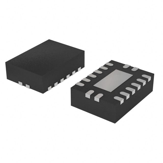
Package
The 74VHC595BQ,115 is available in a small-outline package (SOIC) with 16 pins. This package offers ease of handling and compatibility with standard PCB manufacturing processes.
Essence
The essence of the 74VHC595BQ,115 lies in its ability to efficiently shift and control data across multiple output pins, enabling simplified interfacing with external devices.
Packaging/Quantity
The 74VHC595BQ,115 is typically sold in reels or tubes, containing a quantity of 250 or 2,500 units per package.
Specifications
- Supply Voltage Range: 2V to 5.5V
- Operating Temperature Range: -40°C to +125°C
- Maximum Clock Frequency: 100 MHz
- Number of Output Pins: 8
- Input/Output Logic Compatibility: TTL and CMOS
Detailed Pin Configuration
The 74VHC595BQ,115 has a total of 16 pins. The following table provides a detailed pin configuration:
| Pin Number | Pin Name | Description | |------------|----------|-------------| | 1 | QH' | Serial Output (Inverted) | | 2 | QH | Serial Output | | 3 | QA | Parallel Output A | | 4 | QB | Parallel Output B | | 5 | QC | Parallel Output C | | 6 | QD | Parallel Output D | | 7 | QE | Parallel Output E | | 8 | QF | Parallel Output F | | 9 | QG | Parallel Output G | | 10 | QH | Parallel Output H | | 11 | SER | Serial Data Input | | 12 | RCLK | Register Clock Input | | 13 | SRCLK | Shift Register Clock Input | | 14 | OE | Output Enable Input | | 15 | SRCLR | Shift Register Clear Input | | 16 | VCC | Supply Voltage | | 17 | GND | Ground |
Functional Features
- Serial-to-parallel conversion: The 74VHC595BQ,115 can convert serial data input into parallel outputs.
- Cascade capability: Multiple ICs can be cascaded to increase the number of output pins.
- Output enable control: The OE pin allows for enabling or disabling the outputs.
- Shift register clearing: The SRCLR pin clears the shift register, resetting all outputs to a known state.
Advantages and Disadvantages
Advantages
- Simplified interfacing: The IC reduces the number of pins required on a microcontroller or other digital devices to control multiple outputs.
- High-speed operation: It operates at high clock frequencies, enabling efficient data shifting.
- Low power consumption: The IC is designed to minimize power usage, making it suitable for battery-powered applications.
Disadvantages
- Limited output current: The IC has a limited current sourcing/sinking capability per output pin.
- Requires additional components: External resistors and capacitors may be needed for proper operation in certain applications.
Working Principles
The 74VHC595BQ,115 is based on the principle of serial-in, parallel-out (SIPO) shifting. It receives serial data through the SER pin and shifts it into an internal shift register upon each rising edge of the SRCLK input. The parallel outputs reflect the contents of the shift register and can be latched to the output pins using the RCLK signal. The OE pin allows for enabling or disabling the outputs, while the SRCLR pin clears the shift register, resetting all outputs to a known state.
Detailed Application Field Plans
The 74VHC595BQ,115 finds applications in various fields, including but not limited to: 1.
רשום 10 שאלות ותשובות נפוצות הקשורות ליישום של 74VHC595BQ,115 בפתרונות טכניים
Sure! Here are 10 common questions and answers related to the application of 74VHC595BQ,115 in technical solutions:
Q: What is the 74VHC595BQ,115? A: The 74VHC595BQ,115 is a shift register with an output storage register that can be used in various digital applications.
Q: What is the maximum operating voltage for the 74VHC595BQ,115? A: The maximum operating voltage for the 74VHC595BQ,115 is typically 5.5V.
Q: How many bits can the 74VHC595BQ,115 store? A: The 74VHC595BQ,115 can store 8 bits of data.
Q: Can the 74VHC595BQ,115 be cascaded to increase the number of bits stored? A: Yes, multiple 74VHC595BQ,115 chips can be cascaded together to increase the number of bits stored.
Q: What is the maximum clock frequency supported by the 74VHC595BQ,115? A: The maximum clock frequency supported by the 74VHC595BQ,115 is typically around 100 MHz.
Q: Can the 74VHC595BQ,115 be used for driving LEDs? A: Yes, the 74VHC595BQ,115 can be used to drive LEDs by connecting them to the output pins.
Q: Does the 74VHC595BQ,115 require external pull-up resistors for its inputs? A: No, the 74VHC595BQ,115 has internal pull-up resistors on its inputs, so external pull-up resistors are not necessary.
Q: Can the 74VHC595BQ,115 be used in both parallel and serial data transfer modes? A: Yes, the 74VHC595BQ,115 can be used in both parallel and serial data transfer modes, depending on the application requirements.
Q: What is the power supply voltage range for the 74VHC595BQ,115? A: The power supply voltage range for the 74VHC595BQ,115 is typically between 2V and 5.5V.
Q: Is the 74VHC595BQ,115 compatible with other logic families? A: Yes, the 74VHC595BQ,115 is compatible with a wide range of logic families, including CMOS, TTL, and LSTTL.
Please note that the answers provided here are general and may vary depending on the specific datasheet and manufacturer's specifications for the 74VHC595BQ,115.