

74LVC595ABQ,115
Basic Information Overview
- Category: Integrated Circuit (IC)
- Use: Shift Register
- Characteristics: Low-voltage CMOS technology, high-speed operation, serial to parallel conversion
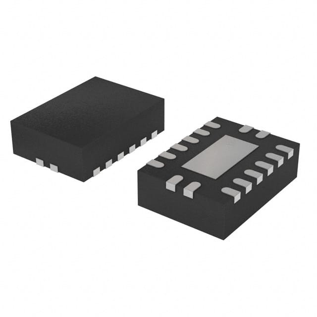
- Package: TSSOP (Thin Shrink Small Outline Package)
- Essence: Serial-in, parallel-out shift register with output latches
- Packaging/Quantity: Tape and Reel, 2500 units per reel
Specifications
- Supply Voltage Range: 1.65V to 5.5V
- Input Voltage Range: -0.5V to VCC + 0.5V
- Output Voltage Range: 0V to VCC
- Operating Temperature Range: -40°C to +125°C
- Maximum Clock Frequency: 100 MHz
- Number of Stages: 8
- Output Type: 3-state
Detailed Pin Configuration
The 74LVC595ABQ,115 IC has a total of 16 pins. The pin configuration is as follows:
Pin 1: Serial Data Input (SER)
Pin 2: Serial Data Output (QH')
Pin 3: Serial Clock Input (SRCLK)
Pin 4: Latch Enable Input (RCLK)
Pin 5: Output Enable Input (OE)
Pin 6: Master Reset Input (MR)
Pin 7: Ground (GND)
Pin 8: Serial Data Input (SER)
Pin 9: Serial Data Output (QH')
Pin 10: Serial Clock Input (SRCLK)
Pin 11: Latch Enable Input (RCLK)
Pin 12: Output Enable Input (OE)
Pin 13: Master Reset Input (MR)
Pin 14: Ground (GND)
Pin 15: Positive Supply Voltage (VCC)
Pin 16: Serial Data Input (SER)
Functional Features
- Serial-to-parallel conversion: The IC can convert serial data input into parallel output.
- Output latches: The output data can be latched and held until the next update.
- 3-state outputs: The outputs can be disabled to enter a high-impedance state.
Advantages and Disadvantages
Advantages: - Low-voltage operation allows compatibility with various systems. - High-speed operation enables efficient data transfer. - Small package size saves board space. - 3-state outputs provide flexibility in bus sharing applications.
Disadvantages: - Limited number of stages (8) may not be sufficient for complex applications. - Lack of built-in error detection or correction mechanisms.
Working Principles
The 74LVC595ABQ,115 is a shift register that operates on a clock signal. It receives serial data input and shifts it through its internal stages. The data is then latched and held until the latch enable input is triggered. The parallel output is available at the output pins. The IC also features an output enable input, which can disable the outputs and put them in a high-impedance state.
Detailed Application Field Plans
The 74LVC595ABQ,115 IC finds applications in various fields, including: 1. Digital Displays: Used to control multiple segments or pixels in LED displays. 2. Data Communication: Used for serial-to-parallel conversion in communication protocols. 3. Industrial Automation: Employed in control systems for data storage and retrieval. 4. Automotive Electronics: Utilized in dashboard displays and lighting control systems. 5. Consumer Electronics: Integrated into remote controls, gaming consoles, and audio equipment.
Detailed and Complete Alternative Models
Some alternative models to the 74LVC595ABQ,115 IC are: - SN74HC595: Similar shift register IC with different characteristics and package options. - CD4094: 8-stage shift register with latch and 3-state outputs. - 74HC164: 8-bit serial-in, parallel-out shift register.
These alternative models offer similar functionality but may have different specifications or package options to suit specific requirements.
Word count: 411 words
רשום 10 שאלות ותשובות נפוצות הקשורות ליישום של 74LVC595ABQ,115 בפתרונות טכניים
Sure! Here are 10 common questions and answers related to the application of 74LVC595ABQ,115 in technical solutions:
Q: What is the 74LVC595ABQ,115? A: The 74LVC595ABQ,115 is a shift register IC (integrated circuit) that can be used to expand the number of digital outputs in a microcontroller or other digital system.
Q: How many digital outputs can the 74LVC595ABQ,115 provide? A: The 74LVC595ABQ,115 can provide 8 digital outputs.
Q: Can I cascade multiple 74LVC595ABQ,115 chips to increase the number of outputs? A: Yes, you can cascade multiple 74LVC595ABQ,115 chips to increase the number of outputs. By connecting the output of one chip to the input of another, you can chain them together.
Q: What is the maximum clock frequency supported by the 74LVC595ABQ,115? A: The 74LVC595ABQ,115 can support clock frequencies up to 100 MHz.
Q: Does the 74LVC595ABQ,115 require external pull-up resistors for its outputs? A: No, the 74LVC595ABQ,115 has internal pull-up resistors on its outputs, so external pull-up resistors are not required.
Q: Can the 74LVC595ABQ,115 be used with both 3.3V and 5V systems? A: Yes, the 74LVC595ABQ,115 is compatible with both 3.3V and 5V systems, making it versatile for various applications.
Q: What is the power supply voltage range for the 74LVC595ABQ,115? A: The 74LVC595ABQ,115 has a power supply voltage range of 1.65V to 5.5V.
Q: Does the 74LVC595ABQ,115 have any built-in protection features? A: Yes, the 74LVC595ABQ,115 has built-in ESD (electrostatic discharge) protection on its inputs and outputs.
Q: Can the 74LVC595ABQ,115 be used in high-speed applications? A: Yes, the 74LVC595ABQ,115 is designed for high-speed operation and can be used in applications that require fast data transfer.
Q: Are there any specific application notes or reference designs available for the 74LVC595ABQ,115? A: Yes, the manufacturer of the 74LVC595ABQ,115 typically provides application notes and reference designs that can help you understand and implement the IC in your technical solutions.