

ראה מפרטים לפרטי מוצר.
74LVC4245APW-Q100J
Basic Information Overview
- Category: Integrated Circuit (IC)
- Use: Level Shifter and Bus Transceiver
- Characteristics: High-speed, low-voltage, bidirectional voltage translation between different logic levels
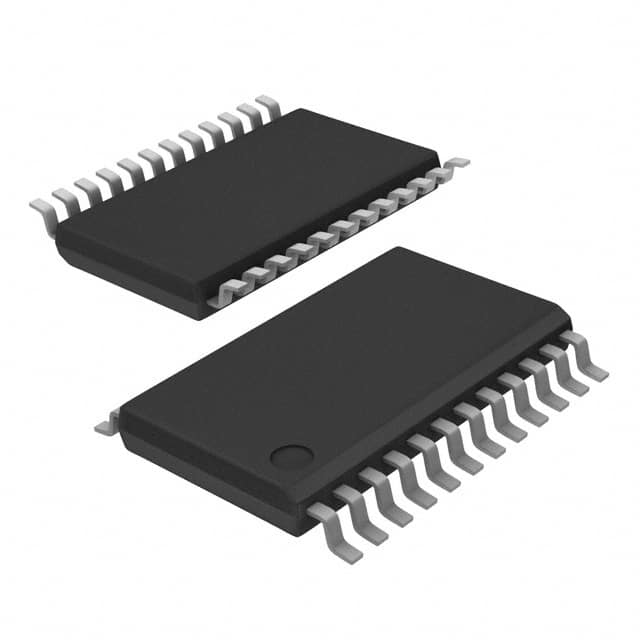
- Package: TSSOP (Thin Shrink Small Outline Package)
- Essence: Voltage level shifting and bus transceiver functionality in a single IC
- Packaging/Quantity: Tape and Reel, 2500 pieces per reel
Specifications
- Supply Voltage Range: 1.2V to 3.6V
- Logic Voltage Levels: 1.2V to 3.6V
- Input/Output Voltage Levels: 1.2V to 3.6V
- Maximum Data Rate: 400 Mbps
- Number of Channels: 8
- Input/Output Capacitance: 4 pF
- Operating Temperature Range: -40°C to +125°C
Detailed Pin Configuration
The 74LVC4245APW-Q100J has a total of 20 pins. The pin configuration is as follows:
- OE (Output Enable) 1
- A1 (Channel 1 Control Input)
- I/O1 (Channel 1 Bidirectional I/O)
- GND (Ground)
- I/O2 (Channel 2 Bidirectional I/O)
- A2 (Channel 2 Control Input)
- VCC (Supply Voltage)
- B1 (Channel 1 Control Input)
- I/O3 (Channel 3 Bidirectional I/O)
- B2 (Channel 2 Control Input)
- I/O4 (Channel 4 Bidirectional I/O)
- GND (Ground)
- I/O5 (Channel 5 Bidirectional I/O)
- B3 (Channel 3 Control Input)
- I/O6 (Channel 6 Bidirectional I/O)
- VCC (Supply Voltage)
- A3 (Channel 3 Control Input)
- I/O7 (Channel 7 Bidirectional I/O)
- A4 (Channel 4 Control Input)
- OE (Output Enable) 2
Functional Features
- Bidirectional voltage translation between different logic levels
- Automatic direction sensing and control
- High-speed operation with data rates up to 400 Mbps
- Low power consumption
- 5V tolerant inputs for easy interfacing with different logic families
- ESD protection on all inputs and outputs
- Schmitt-trigger action on all inputs for noise immunity
Advantages and Disadvantages
Advantages: - Simplifies level shifting and bus transceiver design - Saves board space by integrating multiple functions into a single IC - High-speed operation allows for efficient data transfer - Wide supply voltage range enables compatibility with various systems - ESD protection ensures robustness in harsh environments
Disadvantages: - Limited number of channels (8 in this case) - May not be suitable for applications requiring a higher number of channels
Working Principles
The 74LVC4245APW-Q100J operates by receiving input signals from one logic level and translating them to another logic level. It automatically senses the direction of data flow and controls the bidirectional voltage translation accordingly. The IC uses internal circuitry to ensure fast and reliable data transfer between different logic levels.
Detailed Application Field Plans
The 74LVC4245APW-Q100J is commonly used in various applications, including but not limited to: - Level shifting between different voltage domains in mixed-voltage systems - Bus transceiver for communication interfaces such as UART, SPI, and I2C - Logic level conversion in battery-powered devices with low-voltage requirements - Interface between microcontrollers and peripheral devices operating at different logic levels
Detailed and Complete Alternative Models
Some alternative models that offer similar functionality to the 74LVC4245APW-Q100J include: - SN74LVC4245A from Texas Instruments - MC74VHC245 from ON Semiconductor - 74HCT245 from NXP Semiconductors - CD74HCT245 from Texas Instruments - 74LVCH245A from Nexperia
These alternative models provide comparable voltage level shifting and bus transceiver capabilities, but designers should carefully consider their specific requirements and select the most suitable option based on factors such as supply voltage range, data rate, package type, and availability.
Word count: 529 words
רשום 10 שאלות ותשובות נפוצות הקשורות ליישום של 74LVC4245APW-Q100J בפתרונות טכניים
Sure! Here are 10 common questions and answers related to the application of 74LVC4245APW-Q100J in technical solutions:
Q: What is the purpose of the 74LVC4245APW-Q100J? A: The 74LVC4245APW-Q100J is a bidirectional voltage level translator used for converting signals between different voltage domains.
Q: What voltage levels can the 74LVC4245APW-Q100J handle? A: It can handle voltage levels from 1.2V to 3.6V on the A-side and 1.65V to 5.5V on the B-side.
Q: How many channels does the 74LVC4245APW-Q100J have? A: It has 8 bidirectional channels, allowing for simultaneous translation of multiple signals.
Q: Can the 74LVC4245APW-Q100J be used for level shifting between different logic families? A: Yes, it can be used for level shifting between CMOS, TTL, and other logic families.
Q: What is the maximum data rate supported by the 74LVC4245APW-Q100J? A: It supports data rates up to 400 Mbps, making it suitable for high-speed applications.
Q: Does the 74LVC4245APW-Q100J require external pull-up or pull-down resistors? A: No, it has built-in pull-up and pull-down resistors, simplifying the design.
Q: Can the 74LVC4245APW-Q100J be used for bi-directional communication? A: Yes, it supports bidirectional data flow, allowing for communication in both directions.
Q: What is the power supply voltage range for the 74LVC4245APW-Q100J? A: It operates with a power supply voltage range of 1.2V to 3.6V.
Q: Is the 74LVC4245APW-Q100J suitable for automotive applications? A: Yes, it is designed to meet the requirements of the automotive industry and is qualified to the AEC-Q100 standard.
Q: Can the 74LVC4245APW-Q100J be used in battery-powered devices? A: Yes, it has low power consumption and can be used in battery-powered applications.
Please note that these answers are general and may vary depending on the specific application and requirements.