

AGL1000V5-FG144I
Product Overview
Category
The AGL1000V5-FG144I belongs to the category of Field Programmable Gate Arrays (FPGAs).
Use
This FPGA is primarily used for digital logic design and implementation in various electronic systems.
Characteristics
- High-performance programmable logic device
- Offers flexibility and reconfigurability
- Enables rapid prototyping and development of complex digital circuits
- Supports a wide range of applications
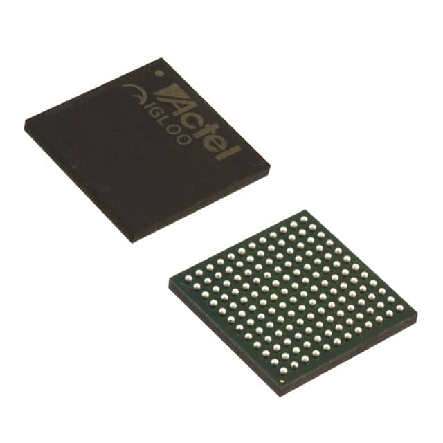
Package
The AGL1000V5-FG144I comes in a compact and durable package, ensuring easy handling and protection during transportation and installation.
Essence
The essence of this FPGA lies in its ability to provide a versatile platform for implementing custom digital designs, allowing for efficient and cost-effective solutions in various industries.
Packaging/Quantity
Each package of AGL1000V5-FG144I contains one FPGA unit.
Specifications
- Model: AGL1000V5-FG144I
- Family: AGL1000
- Package Type: FG144
- Number of Pins: 144
- Operating Voltage: 3.3V
- Logic Cells: 1000
- Maximum Frequency: 250 MHz
- I/O Standards: LVCMOS, LVTTL, SSTL, HSTL, LVDS, RSDS, etc.
- Configuration Memory: Flash-based
Detailed Pin Configuration
The pin configuration of AGL1000V5-FG144I is as follows:
| Pin Number | Pin Name | Description | |------------|----------|-------------| | 1 | VCCIO | Power supply voltage for I/O banks | | 2 | GND | Ground reference | | 3 | IOB0 | General-purpose I/O pin | | ... | ... | ... | | 144 | IOB143 | General-purpose I/O pin |
Functional Features
- High-speed and low-power operation
- Configurable I/O standards for compatibility with various interfaces
- Built-in memory blocks for efficient data storage and retrieval
- Dedicated clock management resources for precise timing control
- Support for advanced debugging and verification features
- Extensive library of pre-designed intellectual property (IP) cores
Advantages and Disadvantages
Advantages
- Flexibility in design and reconfiguration
- Rapid prototyping and time-to-market advantage
- High-performance computing capabilities
- Cost-effective solution for complex digital designs
- Availability of extensive support and documentation
Disadvantages
- Steep learning curve for beginners
- Limited availability of specialized technical expertise
- Higher cost compared to traditional fixed-function integrated circuits
Working Principles
The AGL1000V5-FG144I FPGA operates based on the principles of configurable logic. It consists of an array of programmable logic cells interconnected through configurable routing resources. The logic cells can be programmed to implement desired digital functions, while the routing resources allow for interconnection between these cells. The configuration memory stores the user-defined logic configuration, which can be loaded during startup or dynamically modified during runtime.
Detailed Application Field Plans
The AGL1000V5-FG144I FPGA finds applications in various fields, including:
- Telecommunications: Used in base stations, network switches, and routers for high-speed data processing and protocol handling.
- Automotive: Employed in advanced driver-assistance systems (ADAS), infotainment systems, and engine control units (ECUs) for real-time signal processing and control.
- Aerospace and Defense: Utilized in radar systems, avionics, and military communication equipment for high-performance signal processing and encryption.
- Industrial Automation: Integrated into programmable logic controllers (PLCs), motor control systems, and robotics for precise control and monitoring.
- Medical Devices: Incorporated in medical imaging equipment, patient monitoring systems, and laboratory instruments for data acquisition and processing.
Detailed and Complete Alternative Models
AGL600V2-FG256I
- Family: AGL600
- Package Type: FG256
- Number of Pins: 256
- Logic Cells: 600
- Operating Voltage: 3.3V
- Maximum Frequency: 200 MHz
AGL2000V7-FG484I
- Family: AGL2000
- Package Type: FG484
- Number of Pins: 484
- Logic Cells: 2000
- Operating Voltage: 1.8V
- Maximum Frequency: 300 MHz
AGL5000V10-FG900I
- Family: AGL5000
- Package Type: FG900
- Number of Pins: 900
- Logic Cells: 500
רשום 10 שאלות ותשובות נפוצות הקשורות ליישום של AGL1000V5-FG144I בפתרונות טכניים
Sure! Here are 10 common questions and answers related to the application of AGL1000V5-FG144I in technical solutions:
1. What is the AGL1000V5-FG144I? The AGL1000V5-FG144I is a specific model of Field Programmable Gate Array (FPGA) manufactured by a company called AGL. It is designed for use in various technical solutions.
2. What are the key features of the AGL1000V5-FG144I? Some key features of the AGL1000V5-FG144I include 1000 logic cells, support for up to 144 I/O pins, and field programmability, allowing users to configure the FPGA according to their specific requirements.
3. In what applications can the AGL1000V5-FG144I be used? The AGL1000V5-FG144I can be used in a wide range of applications such as industrial automation, robotics, telecommunications, medical devices, and automotive systems, among others.
4. How does the AGL1000V5-FG144I enhance technical solutions? The AGL1000V5-FG144I enhances technical solutions by providing customizable hardware acceleration, improved performance, reduced power consumption, and increased flexibility compared to traditional microcontrollers or processors.
5. Can the AGL1000V5-FG144I be programmed using a high-level language? Yes, the AGL1000V5-FG144I can be programmed using high-level languages like VHDL or Verilog, which allow designers to describe the desired functionality of the FPGA at a higher level of abstraction.
6. Is the AGL1000V5-FG144I suitable for real-time applications? Yes, the AGL1000V5-FG144I is suitable for real-time applications as it offers fast response times and deterministic behavior, making it ideal for applications that require precise timing or control.
7. Can the AGL1000V5-FG144I interface with other components or devices? Yes, the AGL1000V5-FG144I can interface with other components or devices through its I/O pins, allowing it to communicate with sensors, actuators, memory modules, and other peripherals.
8. What development tools are available for programming the AGL1000V5-FG144I? AGL provides a range of development tools, including software development kits (SDKs), integrated development environments (IDEs), and simulation tools, to facilitate the programming and testing of the AGL1000V5-FG144I.
9. Can the AGL1000V5-FG144I be reprogrammed after deployment? Yes, the AGL1000V5-FG144I is field programmable, meaning it can be reprogrammed even after it has been deployed in a system. This allows for flexibility and adaptability in changing requirements or bug fixes.
10. Are there any limitations or considerations when using the AGL1000V5-FG144I? Some considerations when using the AGL1000V5-FG144I include power consumption, heat dissipation, and the need for proper grounding and signal integrity practices. Additionally, the number of logic cells and I/O pins may limit the complexity of designs that can be implemented on this specific FPGA model.