

A42MX09-1PQG100
Product Overview
Category
A42MX09-1PQG100 belongs to the category of Field Programmable Gate Arrays (FPGAs).
Use
This product is primarily used in digital logic circuits for various applications such as telecommunications, automotive, industrial control systems, and consumer electronics.
Characteristics
- High-performance FPGA with advanced programmable logic capabilities.
- Offers a wide range of configurable logic blocks and input/output resources.
- Provides flexibility in designing complex digital systems.
- Supports reprogramming, allowing for iterative development and customization.
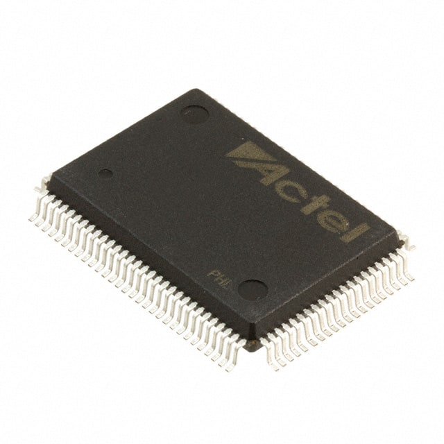
Package
A42MX09-1PQG100 is available in a compact and durable package suitable for surface mount technology (SMT) assembly. The package ensures reliable performance and easy integration into electronic circuit boards.
Essence
The essence of A42MX09-1PQG100 lies in its ability to provide a versatile and customizable solution for implementing digital logic circuits. It enables designers to create complex systems with high levels of functionality and performance.
Packaging/Quantity
This product is typically packaged in reels or trays, depending on the manufacturer's specifications. The quantity per package may vary, but it is commonly available in quantities suitable for both prototyping and large-scale production.
Specifications
- Model: A42MX09-1PQG100
- Logic Elements: 9,600
- Maximum Frequency: 250 MHz
- Embedded Memory: Up to 2,048 Kbits
- I/O Pins: 100
- Operating Voltage: 3.3V
- Package Type: PQG100
Detailed Pin Configuration
The pin configuration of A42MX09-1PQG100 is as follows:
| Pin Number | Pin Name | Description | |------------|----------|-------------| | 1 | VCC | Power Supply Voltage | | 2 | GND | Ground | | 3 | IO1 | Input/Output Pin 1 | | ... | ... | ... | | 100 | IO100 | Input/Output Pin 100 |
Functional Features
- High-speed and high-density programmable logic elements.
- Flexible I/O resources for interfacing with external devices.
- On-chip memory blocks for efficient data storage.
- Dedicated clock management circuitry for precise timing control.
- Built-in support for various communication protocols.
Advantages and Disadvantages
Advantages
- Versatile and customizable solution for digital logic design.
- Enables rapid prototyping and iterative development.
- Offers high-performance capabilities for demanding applications.
- Supports reprogramming, allowing for system upgrades and modifications.
Disadvantages
- Requires expertise in FPGA programming and design.
- Higher cost compared to fixed-function integrated circuits.
- Limited availability of alternative models from different manufacturers.
Working Principles
A42MX09-1PQG100 operates based on the principles of field-programmable gate arrays. It consists of configurable logic blocks (CLBs), interconnect resources, I/O buffers, and other supporting components. The CLBs can be programmed to implement various logic functions, while the interconnect resources facilitate the routing of signals between different blocks. The I/O buffers enable communication with external devices.
The working principle involves configuring the FPGA using a hardware description language (HDL) or a graphical design tool. The desired functionality is defined through the programming of CLBs and interconnections. Once programmed, the FPGA executes the specified logic operations, enabling the desired digital system to function.
Detailed Application Field Plans
A42MX09-1PQG100 finds applications in various fields, including:
- Telecommunications: Used in network routers, switches, and base stations for high-speed data processing and protocol handling.
- Automotive: Employed in automotive control systems for functions like engine management, advanced driver-assistance systems (ADAS), and infotainment.
- Industrial Control Systems: Utilized in programmable logic controllers (PLCs) and automation systems for process control, monitoring, and data acquisition.
- Consumer Electronics: Integrated into devices such as gaming consoles, set-top boxes, and multimedia players to enable complex functionality and connectivity.
Detailed and Complete Alternative Models
While A42MX09-1PQG100 is a reliable FPGA, there are alternative models available from different manufacturers that offer similar capabilities. Some notable alternatives include:
- Xilinx Spartan-6 FPGA
- Intel (Altera) Cyclone V FPGA
- Lattice ECP5 FPGA
- Microchip PolarFire FPGA
These alternative models provide a range of options with varying performance, capacity, and cost considerations, allowing designers to choose the most suitable FPGA for their specific requirements.
Word count: 650 words
רשום 10 שאלות ותשובות נפוצות הקשורות ליישום של A42MX09-1PQG100 בפתרונות טכניים
Sure! Here are 10 common questions and answers related to the application of A42MX09-1PQG100 in technical solutions:
1. What is the A42MX09-1PQG100? - The A42MX09-1PQG100 is a specific model of programmable logic device (PLD) manufactured by Microsemi Corporation.
2. What are the key features of the A42MX09-1PQG100? - The A42MX09-1PQG100 offers 9,600 usable gates, 192 macrocells, and 96 I/O pins. It operates at a maximum frequency of 133 MHz and supports various I/O standards.
3. What are some typical applications for the A42MX09-1PQG100? - The A42MX09-1PQG100 can be used in a wide range of applications, including industrial control systems, telecommunications equipment, automotive electronics, and consumer electronics.
4. How does the A42MX09-1PQG100 differ from other PLDs? - The A42MX09-1PQG100 stands out due to its low power consumption, high performance, and flexibility. It also offers non-volatile configuration memory, which allows it to retain its programming even when powered off.
5. What development tools are available for programming the A42MX09-1PQG100? - Microsemi provides a comprehensive suite of development tools, including software design tools, programming hardware, and simulation environments, to facilitate the programming and testing of the A42MX09-1PQG100.
6. Can the A42MX09-1PQG100 be reprogrammed after deployment? - Yes, the A42MX09-1PQG100 supports in-system programming (ISP), which allows for reprogramming of the device even after it has been deployed in a system.
7. What are the power supply requirements for the A42MX09-1PQG100? - The A42MX09-1PQG100 requires a single power supply voltage of 3.3V, making it compatible with standard power sources used in most electronic systems.
8. Can the A42MX09-1PQG100 interface with other components or devices? - Yes, the A42MX09-1PQG100 supports various I/O standards, such as LVCMOS, LVTTL, and SSTL, allowing it to interface with a wide range of components and devices.
9. Are there any limitations or considerations when using the A42MX09-1PQG100? - Some considerations include the maximum operating frequency, available resources (gates, macrocells), and the need for external memory if additional storage is required.
10. Where can I find more information about the A42MX09-1PQG100? - You can find detailed technical documentation, datasheets, application notes, and support resources on Microsemi's official website or by contacting their customer support team.