

A3PN015-2QNG68I
Product Overview
Category
A3PN015-2QNG68I belongs to the category of programmable logic devices (PLDs).
Use
This product is primarily used in digital circuit design and implementation. It provides a flexible and customizable solution for various applications.
Characteristics
- Programmable: The A3PN015-2QNG68I can be programmed to perform specific functions based on the user's requirements.
- High Integration: It offers a high level of integration, allowing multiple functions to be implemented within a single device.
- Versatile: This PLD supports a wide range of applications due to its programmability.
- Low Power Consumption: The A3PN015-2QNG68I is designed to operate efficiently with low power consumption.
Package
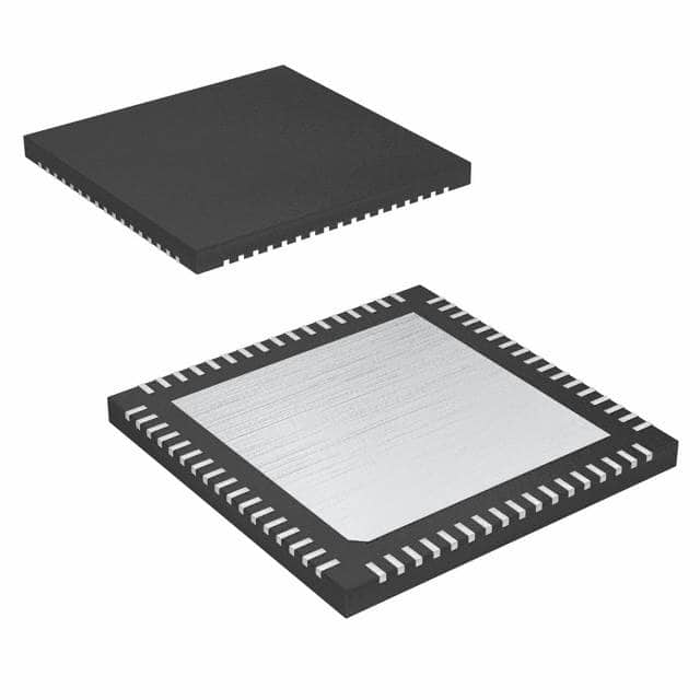
The A3PN015-2QNG68I is available in a compact quad flat no-lead (QFN) package.
Essence
The essence of the A3PN015-2QNG68I lies in its ability to provide a reconfigurable hardware platform that enables users to implement custom digital logic designs.
Packaging/Quantity
This product is typically packaged in reels or trays, with quantities varying depending on customer requirements.
Specifications
- Model: A3PN015-2QNG68I
- Logic Cells: 1500
- I/O Pins: 68
- Operating Voltage: 1.2V
- Speed Grade: -2
- Package Type: QFN
- Temperature Range: -40°C to +85°C
Detailed Pin Configuration
The A3PN015-2QNG68I has a total of 68 I/O pins. The pin configuration is as follows:
(Pin Number) - (Pin Name) 1 - IO0 2 - IO1 3 - IO2 ... 68 - IO67
Functional Features
- Reconfigurability: The A3PN015-2QNG68I can be reprogrammed multiple times, allowing for design changes and updates.
- High-Speed Operation: This PLD offers fast operation speeds, making it suitable for time-critical applications.
- Design Flexibility: Users can implement complex digital logic designs using the available logic cells and I/O pins.
- Integration Capability: The A3PN015-2QNG68I can integrate multiple functions into a single device, reducing the need for additional components.
Advantages and Disadvantages
Advantages
- Customizability: The A3PN015-2QNG68I allows users to create tailored solutions for their specific application needs.
- Cost-Effective: By eliminating the need for dedicated hardware components, this PLD can reduce overall system costs.
- Time-Saving: The reprogrammable nature of the A3PN015-2QNG68I enables faster prototyping and development cycles.
Disadvantages
- Learning Curve: Utilizing programmable logic devices requires knowledge of hardware description languages and digital circuit design principles.
- Limited Resources: The number of logic cells and I/O pins in the A3PN015-2QNG68I may restrict the complexity of certain designs.
Working Principles
The A3PN015-2QNG68I operates based on the principles of field-programmable gate arrays (FPGAs). It consists of configurable logic blocks (CLBs), interconnect resources, and I/O elements. The CLBs can be programmed to perform various logic functions, while the interconnect resources enable communication between different blocks. The I/O elements facilitate interaction with external devices.
Detailed Application Field Plans
The A3PN015-2QNG68I finds applications in various fields, including: 1. Industrial Automation: It can be used to implement control systems for manufacturing processes. 2. Communication Systems: This PLD enables the development of custom communication protocols and signal processing algorithms. 3. Automotive Electronics: The A3PN015-2QNG68I can be utilized in automotive applications such as engine control units (ECUs) and advanced driver-assistance systems (ADAS). 4. Consumer Electronics: It offers a flexible platform for designing custom digital circuits in devices like smartphones, tablets, and gaming consoles.
Detailed and Complete Alternative Models
- A3P030-VQG100: This model offers a higher logic cell count and more I/O pins compared to the A3PN015-2QNG68I.
- A3P060-VQG100: With increased capacity, this alternative provides additional resources for complex designs.
- A3P125-VQG100: This model offers even greater logic cell count and I/O pin availability, suitable for demanding applications.
These alternative models provide options with varying capabilities to meet different design requirements.
Word Count: 579 words
רשום 10 שאלות ותשובות נפוצות הקשורות ליישום של A3PN015-2QNG68I בפתרונות טכניים
Sure! Here are 10 common questions and answers related to the application of A3PN015-2QNG68I in technical solutions:
Question: What is A3PN015-2QNG68I?
Answer: A3PN015-2QNG68I is a specific model number for a field-programmable gate array (FPGA) manufactured by a company called Xilinx.Question: What is the purpose of using A3PN015-2QNG68I in technical solutions?
Answer: A3PN015-2QNG68I is used to implement digital logic circuits and perform various functions such as data processing, signal processing, and control in technical solutions.Question: What are the key features of A3PN015-2QNG68I?
Answer: Some key features of A3PN015-2QNG68I include low power consumption, high-performance capabilities, reprogrammability, and integration of multiple functions on a single chip.Question: How can A3PN015-2QNG68I be programmed?
Answer: A3PN015-2QNG68I can be programmed using hardware description languages (HDLs) such as VHDL or Verilog, or through graphical programming tools provided by Xilinx.Question: What are some typical applications of A3PN015-2QNG68I?
Answer: A3PN015-2QNG68I can be used in various applications such as industrial automation, telecommunications, automotive systems, medical devices, and aerospace technology.Question: Can A3PN015-2QNG68I be used for real-time data processing?
Answer: Yes, A3PN015-2QNG68I is capable of performing real-time data processing tasks due to its high-speed processing capabilities.Question: Is A3PN015-2QNG68I suitable for low-power applications?
Answer: Yes, A3PN015-2QNG68I is designed to be power-efficient and can be used in low-power applications where energy consumption is a critical factor.Question: Can A3PN015-2QNG68I interface with other electronic components or devices?
Answer: Yes, A3PN015-2QNG68I supports various communication protocols and interfaces such as UART, SPI, I2C, and Ethernet, allowing it to interface with other components or devices.Question: Are there any development tools available for programming and debugging A3PN015-2QNG68I?
Answer: Yes, Xilinx provides a range of development tools like Vivado Design Suite that facilitate programming, simulation, and debugging of A3PN015-2QNG68I-based designs.Question: Can A3PN015-2QNG68I be used in safety-critical applications?
Answer: Yes, A3PN015-2QNG68I can be used in safety-critical applications, but additional measures may need to be taken to ensure compliance with relevant safety standards and regulations.