

RC28F256J3F95A
Product Overview
Category
The RC28F256J3F95A belongs to the category of flash memory chips.
Use
This product is primarily used for data storage in various electronic devices such as smartphones, tablets, digital cameras, and portable media players.
Characteristics
- High storage capacity: The RC28F256J3F95A offers a large storage capacity, allowing users to store a significant amount of data.
- Fast data transfer rate: This flash memory chip provides high-speed data transfer, enabling quick access to stored information.
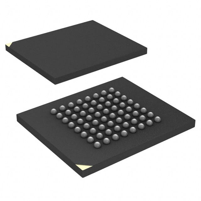
- Compact package: The RC28F256J3F95A comes in a compact package, making it suitable for integration into small-sized electronic devices.
- Reliable performance: With its robust design and advanced technology, this flash memory chip ensures reliable and consistent performance.
- Low power consumption: The RC28F256J3F95A is designed to consume minimal power, contributing to energy efficiency in electronic devices.
Packaging/Quantity
The RC28F256J3F95A is typically packaged in a small form factor, such as a surface-mount device (SMD) package. It is available in various quantities, ranging from individual units to bulk packaging options.
Specifications
- Storage Capacity: 256 megabytes (MB)
- Interface: Serial Peripheral Interface (SPI)
- Operating Voltage: 2.7V - 3.6V
- Data Transfer Rate: Up to 50 megabits per second (Mbps)
- Operating Temperature Range: -40°C to +85°C
- Package Type: Small Outline Integrated Circuit (SOIC)
Detailed Pin Configuration
The RC28F256J3F95A features a specific pin configuration that facilitates its integration into electronic circuits. The following table outlines the pin assignments:
| Pin Number | Pin Name | Function | |------------|----------|----------| | 1 | VCC | Power Supply Voltage | | 2 | GND | Ground | | 3 | CS | Chip Select | | 4 | SCK | Serial Clock | | 5 | SI | Serial Input | | 6 | SO | Serial Output | | 7 | WP# | Write Protect | | 8 | HOLD# | Hold |
Functional Features
- Erase and Program Operations: The RC28F256J3F95A supports both erase and program operations, allowing users to modify the stored data as needed.
- Error Correction Code (ECC): This flash memory chip incorporates ECC algorithms to ensure data integrity and reliability.
- Wear-Leveling Algorithm: To extend the lifespan of the memory cells, the RC28F256J3F95A employs a wear-leveling algorithm that evenly distributes write and erase cycles across the entire chip.
- Security Features: This product includes security features such as hardware-based data protection and encryption mechanisms to safeguard sensitive information.
Advantages and Disadvantages
Advantages
- High storage capacity enables ample data storage.
- Fast data transfer rate allows for quick access to stored information.
- Compact package facilitates integration into small-sized electronic devices.
- Reliable performance ensures consistent operation.
- Low power consumption contributes to energy efficiency.
Disadvantages
- Limited compatibility with certain older device interfaces.
- Relatively higher cost compared to lower-capacity flash memory chips.
Working Principles
The RC28F256J3F95A utilizes the principles of NAND flash memory technology. It stores data in memory cells organized in a grid-like structure, where each cell can hold multiple bits of information. The data is written and read by applying electrical charges to these cells, which represent binary values.
Detailed Application Field Plans
The RC28F256J3F95A finds applications in various electronic devices, including but not limited to: - Smartphones and tablets - Digital cameras - Portable media players - Solid-state drives (SSDs) - Industrial control systems - Automotive electronics
Detailed and Complete Alternative Models
- RC28F256J3D75A: Similar to the RC28F256J3F95A, this model offers a high storage capacity and fast data transfer rate.
- RC28F128J3F95A: This alternative model provides half the storage capacity of the RC28F256J3F95A but retains similar characteristics and features.
- RC28F512J3F95A: With double the storage capacity of the RC28F256J3F95A, this model is suitable for applications requiring more extensive data storage.
These alternative models offer flexibility in choosing the appropriate flash memory chip based on specific requirements.
Word count: 570 words
רשום 10 שאלות ותשובות נפוצות הקשורות ליישום של RC28F256J3F95A בפתרונות טכניים
Sure! Here are 10 common questions and answers related to the application of RC28F256J3F95A in technical solutions:
Q: What is RC28F256J3F95A? A: RC28F256J3F95A is a type of flash memory chip manufactured by Intel.
Q: What is the storage capacity of RC28F256J3F95A? A: RC28F256J3F95A has a storage capacity of 256 megabits (32 megabytes).
Q: What is the interface used for connecting RC28F256J3F95A to a microcontroller or processor? A: RC28F256J3F95A uses a parallel NOR flash interface.
Q: What is the operating voltage range of RC28F256J3F95A? A: RC28F256J3F95A operates at a voltage range of 2.7V to 3.6V.
Q: What is the maximum clock frequency supported by RC28F256J3F95A? A: RC28F256J3F95A supports a maximum clock frequency of 95 MHz.
Q: Can RC28F256J3F95A be used for code execution in embedded systems? A: Yes, RC28F256J3F95A can be used for storing and executing code in embedded systems.
Q: Is RC28F256J3F95A suitable for high-reliability applications? A: Yes, RC28F256J3F95A is designed for high-reliability applications and offers extended temperature ranges and data retention.
Q: Does RC28F256J3F95A support in-system programming (ISP)? A: Yes, RC28F256J3F95A supports in-system programming, allowing for firmware updates without removing the chip from the system.
Q: Can RC28F256J3F95A be used as a boot device in embedded systems? A: Yes, RC28F256J3F95A can be used as a boot device to store the initial boot code of an embedded system.
Q: Are there any specific precautions or considerations when using RC28F256J3F95A in a design? A: It is important to follow the datasheet guidelines provided by Intel for proper power supply decoupling, signal integrity, and timing requirements during the design and layout process.
Please note that these answers are general and may vary depending on the specific application and requirements.