

SY100S331JC
Product Overview
Category
SY100S331JC belongs to the category of integrated circuits (ICs).
Use
This IC is commonly used in electronic devices for signal processing and data transmission.
Characteristics
- High-speed operation
- Low power consumption
- Compact size
- Reliable performance
Package
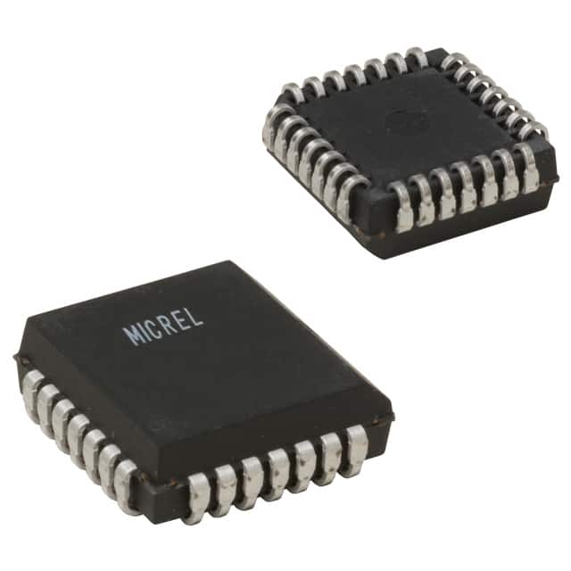
SY100S331JC is available in a small outline integrated circuit (SOIC) package.
Essence
The essence of SY100S331JC lies in its ability to process signals efficiently and transmit data accurately.
Packaging/Quantity
Each package of SY100S331JC contains 25 individual ICs.
Specifications
- Supply Voltage: 3.3V
- Operating Temperature Range: -40°C to +85°C
- Input Voltage Range: 0V to VCC
- Output Voltage Range: 0V to VCC
- Maximum Clock Frequency: 200 MHz
- Power Dissipation: 500 mW
Detailed Pin Configuration
SY100S331JC has a total of 20 pins, which are assigned specific functions as follows:
- CLK (Clock Input)
- GND (Ground)
- Q0 (Output 0)
- Q1 (Output 1)
- Q2 (Output 2)
- Q3 (Output 3)
- Q4 (Output 4)
- Q5 (Output 5)
- Q6 (Output 6)
- Q7 (Output 7)
- Q8 (Output 8)
- Q9 (Output 9)
- Q10 (Output 10)
- Q11 (Output 11)
- Q12 (Output 12)
- Q13 (Output 13)
- Q14 (Output 14)
- Q15 (Output 15)
- VCC (Power Supply)
- GND (Ground)
Functional Features
- High-speed parallel-to-serial conversion
- Serial data output with clock synchronization
- Wide input voltage range
- Low power consumption
- Output enable control for power management
Advantages and Disadvantages
Advantages
- Fast data processing and transmission
- Compact size allows for integration into various electronic devices
- Low power consumption helps conserve energy
- Reliable performance ensures accurate signal processing
Disadvantages
- Limited number of output pins may restrict certain applications
- Requires external clock signal for proper operation
Working Principles
SY100S331JC operates by receiving parallel input data and converting it into a serial data stream. The internal circuitry processes the data at high speed, synchronized with the clock signal. The converted serial data is then transmitted through the output pins.
Detailed Application Field Plans
SY100S331JC finds applications in various fields, including:
- Telecommunications: Used in data communication systems for efficient signal processing and transmission.
- Networking: Integrated into network devices to handle high-speed data transfer.
- Industrial Automation: Employed in industrial control systems for reliable data processing.
- Consumer Electronics: Incorporated into electronic devices such as TVs, set-top boxes, and gaming consoles for enhanced data handling capabilities.
Detailed and Complete Alternative Models
- SY100S331JCTR
- SY100S331JCTR-E3
- SY100S331JCTR-G
These alternative models offer similar functionality and characteristics to SY100S331JC, providing flexibility in choosing the most suitable option for specific applications.
Word count: 515 words
רשום 10 שאלות ותשובות נפוצות הקשורות ליישום של SY100S331JC בפתרונות טכניים
Sure! Here are 10 common questions and answers related to the application of SY100S331JC in technical solutions:
Q: What is SY100S331JC? A: SY100S331JC is a specific integrated circuit (IC) chip designed for various technical applications.
Q: What are the key features of SY100S331JC? A: Some key features of SY100S331JC include low power consumption, high-speed operation, and compatibility with different logic families.
Q: In which technical solutions can SY100S331JC be used? A: SY100S331JC can be used in applications such as data communication systems, clock distribution networks, and digital signal processing.
Q: What is the operating voltage range for SY100S331JC? A: The operating voltage range for SY100S331JC typically falls between 4.5V and 5.5V.
Q: Can SY100S331JC handle high-frequency signals? A: Yes, SY100S331JC is designed to handle high-frequency signals, making it suitable for applications that require fast data transmission.
Q: Does SY100S331JC support multiple input/output channels? A: Yes, SY100S331JC typically supports multiple input/output channels, allowing for versatile connectivity options.
Q: Is SY100S331JC compatible with other logic families? A: Yes, SY100S331JC is generally compatible with various logic families, including TTL and CMOS.
Q: What is the typical power consumption of SY100S331JC? A: The typical power consumption of SY100S331JC is relatively low, making it suitable for power-sensitive applications.
Q: Can SY100S331JC be used in automotive applications? A: Yes, SY100S331JC is often used in automotive applications due to its robustness and ability to withstand harsh operating conditions.
Q: Are there any specific design considerations when using SY100S331JC? A: It is important to consider factors such as signal integrity, power supply stability, and proper grounding techniques when designing with SY100S331JC to ensure optimal performance.
Please note that the answers provided here are general and may vary depending on the specific requirements and datasheet of SY100S331JC.