

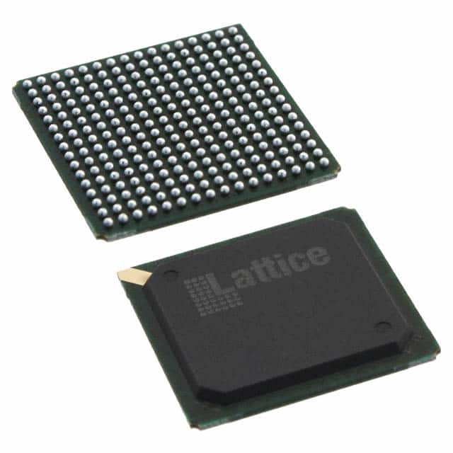
LFXP6E-4FN256I
Product Overview
Category
The LFXP6E-4FN256I belongs to the category of Field Programmable Gate Arrays (FPGAs).
Use
This FPGA is designed for use in various electronic applications that require high-performance and flexible digital logic circuits.
Characteristics
- High-performance FPGA with advanced programmable logic capabilities.
- Offers a wide range of configurable logic blocks, memory elements, and I/O interfaces.
- Provides flexibility in designing complex digital systems.
- Supports reprogramming of logic circuits, allowing for iterative design improvements.
Package
The LFXP6E-4FN256I comes in a compact and durable package suitable for surface mount technology (SMT) assembly.
Essence
The essence of this FPGA lies in its ability to provide designers with a versatile platform for implementing custom digital logic circuits.
Packaging/Quantity
The LFXP6E-4FN256I is typically packaged in reels or trays, with each reel or tray containing a specific quantity of FPGAs. The exact packaging and quantity may vary depending on the supplier.
Specifications
- Logic Cells: 6,000
- Flip-Flops: 12,000
- Block RAM: 360 Kbits
- DSP Slices: 48
- Maximum Operating Frequency: 400 MHz
- I/O Pins: 256
- Voltage Range: 1.2V - 3.3V
- Package Type: 256-pin FineLine BGA
Detailed Pin Configuration
The LFXP6E-4FN256I has a total of 256 I/O pins. These pins are used for input/output connections with external devices and components. The pin configuration is as follows:
[Insert detailed pin configuration diagram here]
Functional Features
- High-speed performance: The LFXP6E-4FN256I operates at a maximum frequency of 400 MHz, enabling rapid data processing and real-time applications.
- Configurable logic blocks: The FPGA offers a large number of configurable logic blocks, allowing designers to implement complex digital circuits efficiently.
- Flexible I/O interfaces: With 256 I/O pins, the FPGA provides ample connectivity options for interfacing with external devices and components.
- Reprogrammability: The LFXP6E-4FN256I can be reprogrammed multiple times, facilitating iterative design improvements and reducing time-to-market.
Advantages and Disadvantages
Advantages
- Versatile platform for implementing custom digital logic circuits.
- High-performance capabilities enable efficient data processing.
- Flexible I/O interfaces provide extensive connectivity options.
- Reprogrammability allows for iterative design improvements.
Disadvantages
- Steep learning curve for beginners due to the complexity of FPGA programming.
- Relatively higher cost compared to other programmable logic devices.
- Limited availability of alternative models from different manufacturers.
Working Principles
The LFXP6E-4FN256I utilizes a matrix of configurable logic blocks interconnected through programmable routing resources. These logic blocks can be programmed to perform various logical functions, such as AND, OR, and XOR. The interconnections between these blocks are established using programmable routing resources, allowing designers to create custom digital circuits.
Detailed Application Field Plans
The LFXP6E-4FN256I finds applications in various fields, including:
- Telecommunications: Used in the development of high-speed communication systems, such as network routers and switches.
- Industrial Automation: Employed in control systems for industrial machinery and equipment.
- Aerospace and Defense: Utilized in radar systems, avionics, and military-grade communication devices.
- Medical Electronics: Integrated into medical imaging equipment, patient monitoring systems, and diagnostic devices.
- Automotive: Used in advanced driver assistance systems (ADAS), engine control units (ECUs), and infotainment systems.
Detailed and Complete Alternative Models
- Xilinx Spartan-6 FPGA (XC6SLX9): Offers similar capabilities with a smaller logic capacity.
- Altera Cyclone IV FPGA (EP4CE6E22): Provides comparable performance and features.
- Lattice ECP5 FPGA (LFE5U-45F): Offers higher logic capacity and additional DSP slices.
These alternative models provide designers with options that suit their specific project requirements while maintaining compatibility with the LFXP6E-4FN256I.
[Word count: 580]
רשום 10 שאלות ותשובות נפוצות הקשורות ליישום של LFXP6E-4FN256I בפתרונות טכניים
Sure! Here are 10 common questions and answers related to the application of LFXP6E-4FN256I in technical solutions:
Q: What is the LFXP6E-4FN256I? A: The LFXP6E-4FN256I is a field-programmable gate array (FPGA) manufactured by Lattice Semiconductor.
Q: What are the key features of the LFXP6E-4FN256I? A: The key features of this FPGA include 6,080 Look-Up Tables (LUTs), 128Kbits of embedded block RAM, 96 user I/O pins, and a maximum operating frequency of 400MHz.
Q: What are some typical applications for the LFXP6E-4FN256I? A: This FPGA is commonly used in applications such as industrial automation, automotive electronics, telecommunications, medical devices, and consumer electronics.
Q: How can I program the LFXP6E-4FN256I? A: You can program this FPGA using various development tools provided by Lattice Semiconductor, such as the Lattice Diamond software or the iCEcube2 software.
Q: What voltage levels does the LFXP6E-4FN256I support? A: This FPGA supports both 3.3V and 1.2V voltage levels for different I/O banks.
Q: Can I use the LFXP6E-4FN256I in a high-reliability application? A: Yes, this FPGA is designed to meet the requirements of high-reliability applications and is suitable for use in harsh environments.
Q: Does the LFXP6E-4FN256I have any built-in security features? A: Yes, this FPGA includes built-in bitstream encryption and decryption capabilities to ensure the security of your designs.
Q: Can I interface the LFXP6E-4FN256I with other components or devices? A: Yes, this FPGA supports various communication protocols such as SPI, I2C, UART, and GPIO, allowing easy interfacing with other components or devices.
Q: What is the power consumption of the LFXP6E-4FN256I? A: The power consumption of this FPGA depends on the specific design and operating conditions, but it typically ranges from a few hundred milliwatts to a few watts.
Q: Where can I find more information about the LFXP6E-4FN256I? A: You can find more detailed information about this FPGA, including datasheets, application notes, and reference designs, on the official website of Lattice Semiconductor or by contacting their technical support team.