

LFXP6E-3QN208C
Product Overview
Category
The LFXP6E-3QN208C belongs to the category of Field-Programmable Gate Arrays (FPGAs).
Use
This FPGA is designed for various applications that require high-performance digital signal processing, such as telecommunications, automotive, industrial automation, and aerospace.
Characteristics
- High-speed performance: The LFXP6E-3QN208C offers fast data processing capabilities, making it suitable for demanding applications.
- Programmability: It can be reprogrammed multiple times, allowing for flexibility in design and functionality.
- Low power consumption: This FPGA is designed to minimize power consumption, making it energy-efficient.
- Compact package: The LFXP6E-3QN208C comes in a small form factor, enabling space-saving integration into electronic systems.
- Robustness: It is built to withstand harsh operating conditions, ensuring reliability and durability.
Package and Quantity
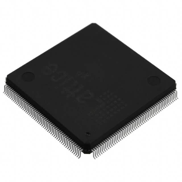
The LFXP6E-3QN208C is available in a Quad Flat No-Lead (QFN) package. Each package contains one unit of the FPGA.
Specifications
- Device family: LatticeXP2
- Logic cells: 6,016
- Look-up tables (LUTs): 12,032
- Flip-flops: 12,032
- Block RAM: 288 Kbits
- Maximum user I/Os: 208
- Operating voltage: 1.2V
- Maximum operating frequency: 400 MHz
- Configuration memory: 4 Mbits
- Package dimensions: 20mm x 20mm
Detailed Pin Configuration
The LFXP6E-3QN208C has a total of 208 pins, each serving a specific function within the FPGA. The pin configuration includes input/output pins, clock pins, power supply pins, and configuration pins. For a detailed pinout diagram, please refer to the manufacturer's datasheet.
Functional Features
- High-speed data processing: The LFXP6E-3QN208C offers fast logic operations, enabling efficient handling of complex algorithms and real-time data.
- Flexible design: With its programmable nature, this FPGA allows for customization and adaptation to specific application requirements.
- On-chip memory: The built-in block RAM provides ample storage capacity for intermediate data and lookup tables, enhancing overall performance.
- I/O versatility: The FPGA supports a wide range of input/output standards, facilitating seamless integration with other electronic components.
- Low power consumption: The LFXP6E-3QN208C is designed to minimize energy usage, making it suitable for battery-powered devices.
Advantages and Disadvantages
Advantages
- High-performance capabilities
- Flexibility in design and functionality
- Energy-efficient operation
- Compact form factor
- Robustness for harsh environments
Disadvantages
- Limited number of user I/Os
- Relatively high cost compared to other FPGA options
- Steeper learning curve for programming and utilization
Working Principles
The LFXP6E-3QN208C operates based on the principles of reconfigurable digital logic. It consists of an array of configurable logic blocks (CLBs) interconnected through programmable routing resources. These CLBs can be programmed to perform various logic functions, allowing for the implementation of complex digital circuits. The FPGA's behavior is determined by the configuration data stored in its non-volatile memory, which can be modified as needed.
Detailed Application Field Plans
The LFXP6E-3QN208C finds applications in diverse fields, including:
- Telecommunications: Used in base stations, routers, and network switches for high-speed data processing and protocol handling.
- Automotive: Employed in advanced driver-assistance systems (ADAS), infotainment systems, and engine control units (ECUs) for real-time data processing and control.
- Industrial Automation: Utilized in programmable logic controllers (PLCs), motor control systems, and robotics for precise control and automation tasks.
- Aerospace: Integrated into avionics systems, satellite communication equipment, and flight control systems to handle complex algorithms and ensure reliable operation.
Detailed and Complete Alternative Models
- Xilinx Spartan-6 XC6SLX9: Offers similar performance and features with a different architecture.
- Intel Cyclone IV EP4CE22: Provides comparable capabilities with a focus on low power consumption.
- Microsemi ProASIC3 A3P060: Offers high-security features along with FPGA functionality.
These alternative models can be considered based on specific project requirements and design constraints.
Word count: 560 words
רשום 10 שאלות ותשובות נפוצות הקשורות ליישום של LFXP6E-3QN208C בפתרונות טכניים
Sure! Here are 10 common questions and answers related to the application of LFXP6E-3QN208C in technical solutions:
Q: What is LFXP6E-3QN208C? A: LFXP6E-3QN208C is a field-programmable gate array (FPGA) manufactured by Lattice Semiconductor.
Q: What are the key features of LFXP6E-3QN208C? A: Some key features of LFXP6E-3QN208C include 6,080 Look-Up Tables (LUTs), 208-pin QFN package, low power consumption, and high-speed performance.
Q: What are the typical applications of LFXP6E-3QN208C? A: LFXP6E-3QN208C is commonly used in various technical solutions such as industrial automation, telecommunications, automotive electronics, medical devices, and consumer electronics.
Q: How can LFXP6E-3QN208C be programmed? A: LFXP6E-3QN208C can be programmed using hardware description languages (HDL) like VHDL or Verilog, or through graphical programming tools provided by Lattice Semiconductor.
Q: What is the power supply requirement for LFXP6E-3QN208C? A: LFXP6E-3QN208C requires a power supply voltage of 1.2V.
Q: Can LFXP6E-3QN208C interface with other components or devices? A: Yes, LFXP6E-3QN208C supports various communication interfaces such as SPI, I2C, UART, and GPIO, allowing it to interface with other components or devices.
Q: What is the maximum operating frequency of LFXP6E-3QN208C? A: The maximum operating frequency of LFXP6E-3QN208C is typically around 400 MHz, depending on the design and implementation.
Q: Does LFXP6E-3QN208C have built-in memory? A: No, LFXP6E-3QN208C does not have built-in memory. However, it can be used to interface with external memory devices if required.
Q: Can LFXP6E-3QN208C be reprogrammed after deployment? A: Yes, LFXP6E-3QN208C is a field-programmable device, which means it can be reprogrammed even after it has been deployed in a system.
Q: Are there any development tools available for LFXP6E-3QN208C? A: Yes, Lattice Semiconductor provides development tools like Lattice Diamond or Lattice Radiant software suites that support the design, simulation, and programming of LFXP6E-3QN208C.
Please note that the answers provided here are general and may vary based on specific requirements and use cases.