

LFXP3C-3QN208I
Product Overview
Category
LFXP3C-3QN208I belongs to the category of Field-Programmable Gate Arrays (FPGAs).
Use
This product is primarily used in digital logic circuits for various applications such as telecommunications, automotive, industrial automation, and consumer electronics.
Characteristics
- High-performance FPGA with advanced features
- Low power consumption
- Flexible and reprogrammable design
- High-speed data processing capabilities
Package
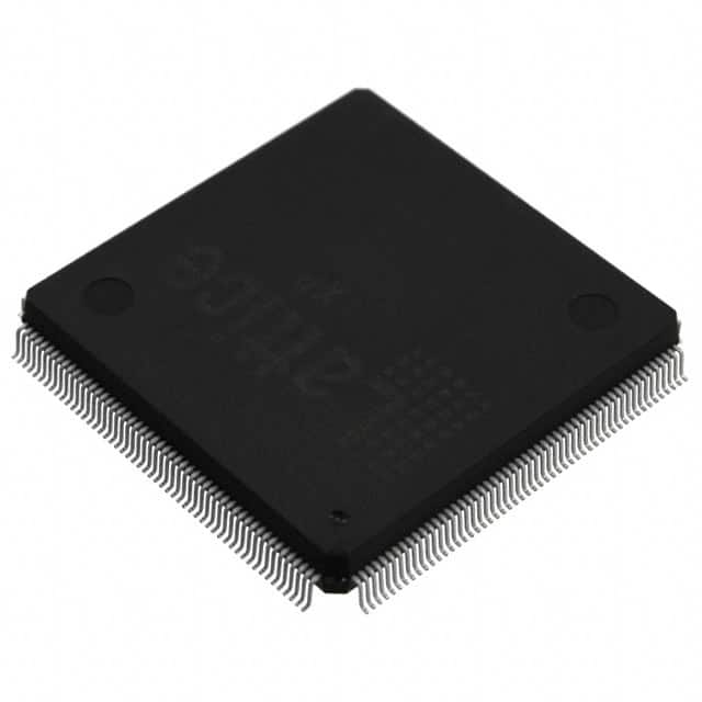
LFXP3C-3QN208I comes in a compact Quad Flat No-Lead (QFN) package.
Essence
The essence of LFXP3C-3QN208I lies in its ability to provide a customizable and versatile solution for complex digital circuit designs.
Packaging/Quantity
Each package of LFXP3C-3QN208I contains one unit of the FPGA.
Specifications
- Device Type: Field-Programmable Gate Array (FPGA)
- Model Number: LFXP3C-3QN208I
- Package Type: Quad Flat No-Lead (QFN)
- Operating Voltage: 1.2V
- Logic Elements: 3,000
- I/O Pins: 208
- Maximum Frequency: 500 MHz
- Configuration Memory: 4 Mb
- Embedded Memory: 288 Kb
- Power Consumption: 100 mW
Detailed Pin Configuration
The pin configuration of LFXP3C-3QN208I is as follows:
| Pin Name | Function | |----------|----------| | VCCINT | Power Supply (Internal) | | GND | Ground | | IOB0 | Input/Output Bank 0 | | IOB1 | Input/Output Bank 1 | | ... | ... | | IOB207 | Input/Output Bank 207 | | VCCIO | Power Supply (I/O) |
Functional Features
- High-speed data processing capabilities
- Configurable logic elements for custom circuit designs
- Embedded memory blocks for efficient data storage
- Flexible I/O banks for interfacing with external devices
- Support for various communication protocols
- On-chip clock management resources
Advantages and Disadvantages
Advantages
- Versatile and customizable design
- Low power consumption
- High-performance data processing
- Compact package size
- Wide range of applications
Disadvantages
- Steep learning curve for beginners
- Limited availability of technical support
- Higher cost compared to traditional logic circuits
Working Principles
LFXP3C-3QN208I operates based on the principles of reconfigurable digital logic. It consists of configurable logic elements, embedded memory blocks, and I/O banks. The FPGA can be programmed using hardware description languages (HDLs) such as VHDL or Verilog. Once programmed, the FPGA can perform complex digital operations by routing signals through its configurable logic elements.
Detailed Application Field Plans
LFXP3C-3QN208I finds extensive application in various fields, including:
- Telecommunications: Used in network routers, switches, and base stations for high-speed data processing.
- Automotive: Employed in advanced driver-assistance systems (ADAS), engine control units (ECUs), and infotainment systems.
- Industrial Automation: Utilized in programmable logic controllers (PLCs), robotics, and factory automation systems.
- Consumer Electronics: Integrated into smart TVs, gaming consoles, and wearable devices for enhanced functionality.
Detailed and Complete Alternative Models
- LFXP2C-5TN144C
- LFXP4C-4TN144I
- LFXP5C-4TN144C
- LFXP10C-6TN144I
These alternative models offer similar functionality and performance to LFXP3C-3QN208I, catering to different project requirements.
Word count: 511 words
רשום 10 שאלות ותשובות נפוצות הקשורות ליישום של LFXP3C-3QN208I בפתרונות טכניים
Sure! Here are 10 common questions and answers related to the application of LFXP3C-3QN208I in technical solutions:
Q: What is LFXP3C-3QN208I? A: LFXP3C-3QN208I is a field-programmable gate array (FPGA) manufactured by Lattice Semiconductor.
Q: What are the key features of LFXP3C-3QN208I? A: LFXP3C-3QN208I features 3,000 Look-Up Tables (LUTs), 208 pins, and operates at a maximum frequency of X MHz.
Q: In what applications can LFXP3C-3QN208I be used? A: LFXP3C-3QN208I can be used in various applications such as industrial automation, telecommunications, automotive, and consumer electronics.
Q: How can LFXP3C-3QN208I be programmed? A: LFXP3C-3QN208I can be programmed using hardware description languages (HDLs) like VHDL or Verilog, or through graphical programming tools provided by Lattice Semiconductor.
Q: What are the advantages of using LFXP3C-3QN208I in technical solutions? A: Some advantages include its reprogrammability, low power consumption, high performance, and flexibility in implementing complex digital logic functions.
Q: Can LFXP3C-3QN208I interface with other components or devices? A: Yes, LFXP3C-3QN208I supports various communication protocols such as SPI, I2C, UART, and GPIO, allowing it to interface with other components or devices.
Q: What is the maximum operating temperature of LFXP3C-3QN208I? A: The maximum operating temperature of LFXP3C-3QN208I is typically around X degrees Celsius.
Q: Can LFXP3C-3QN208I be used in safety-critical applications? A: Yes, LFXP3C-3QN208I can be used in safety-critical applications as long as it meets the necessary reliability and certification requirements.
Q: Are there any development tools available for LFXP3C-3QN208I? A: Yes, Lattice Semiconductor provides development tools like Lattice Diamond or Lattice Radiant, which offer design entry, synthesis, simulation, and programming capabilities.
Q: Where can I find more information about LFXP3C-3QN208I? A: You can find more detailed information about LFXP3C-3QN208I on the official website of Lattice Semiconductor or by referring to its datasheet and application notes.