

LFXP10C-5F256C
Product Overview
Category
The LFXP10C-5F256C belongs to the category of Field-Programmable Gate Arrays (FPGAs).
Use
FPGAs are integrated circuits that can be programmed after manufacturing. The LFXP10C-5F256C is specifically designed for digital logic applications.
Characteristics
- High flexibility and reconfigurability
- Ability to implement complex digital systems
- Low power consumption
- Fast processing speed
- Large number of programmable logic elements
- On-chip memory resources
Package
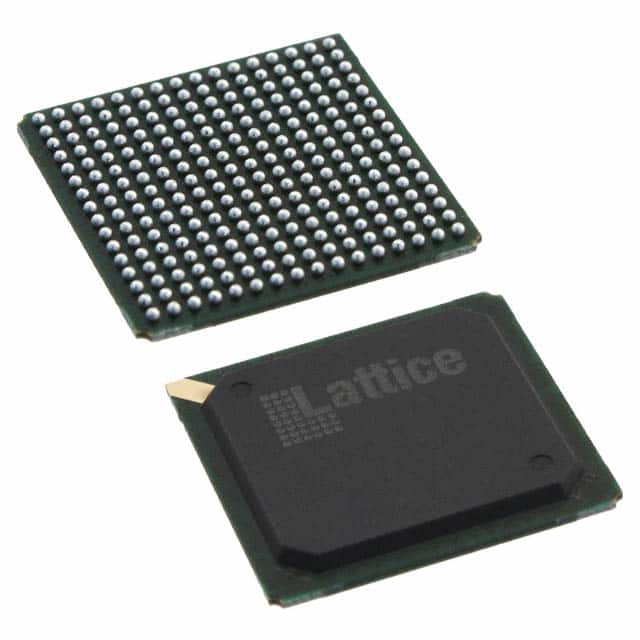
The LFXP10C-5F256C comes in a compact package, suitable for surface mount technology (SMT) assembly.
Essence
The essence of the LFXP10C-5F256C lies in its ability to provide a customizable hardware platform for various digital applications.
Packaging/Quantity
The LFXP10C-5F256C is typically packaged in reels or trays, with a quantity of 250 units per reel/tray.
Specifications
- FPGA Family: LatticeXP2
- Logic Cells: 10,080
- Flip-Flops: 20,160
- Block RAM: 256 Kbits
- Maximum Frequency: 400 MHz
- I/O Pins: 256
- Voltage Range: 1.2V - 3.3V
- Operating Temperature: -40°C to 85°C
Detailed Pin Configuration
The LFXP10C-5F256C has 256 I/O pins, each serving a specific purpose in the overall functionality of the FPGA. For a detailed pin configuration diagram, please refer to the manufacturer's datasheet.
Functional Features
- Configurable logic blocks
- Programmable interconnects
- Dedicated clock management resources
- On-chip memory blocks
- Built-in multipliers and arithmetic functions
- Support for various communication protocols (e.g., SPI, I2C)
Advantages
- Flexibility: The LFXP10C-5F256C allows for easy modification of the hardware design, enabling rapid prototyping and iterative development.
- High Performance: With a maximum frequency of 400 MHz, the FPGA can handle complex digital processing tasks efficiently.
- Low Power Consumption: The LFXP10C-5F256C is designed to minimize power consumption, making it suitable for battery-powered applications.
- Cost-Effective: FPGAs eliminate the need for custom ASICs, reducing development costs and time-to-market.
Disadvantages
- Complexity: Designing and programming FPGAs requires specialized knowledge and expertise.
- Limited Resources: The number of logic cells and memory blocks may not be sufficient for extremely large-scale designs.
- Higher Cost: FPGAs are generally more expensive than traditional microcontrollers or application-specific integrated circuits (ASICs).
Working Principles
The LFXP10C-5F256C operates based on the principles of reconfigurable computing. It consists of configurable logic blocks interconnected through programmable routing resources. The FPGA's functionality is determined by the configuration data loaded into its internal memory.
Detailed Application Field Plans
The LFXP10C-5F256C finds applications in various fields, including: 1. Communications: Implementing digital signal processing algorithms, encryption/decryption, and protocol handling. 2. Industrial Automation: Control systems, motor control, and sensor interfacing. 3. Aerospace and Defense: Radar signal processing, image/video processing, and secure communications. 4. Medical Devices: Image analysis, patient monitoring, and diagnostic equipment. 5. Internet of Things (IoT): Sensor data aggregation, edge computing, and connectivity management.
Detailed and Complete Alternative Models
- Xilinx Spartan-6 XC6SLX9
- Altera Cyclone IV EP4CE6
- Microsemi SmartFusion2 M2S010
- Intel MAX 10 10M08
- QuickLogic EOS S3
These alternative models offer similar functionality and can be considered as alternatives to the LFXP10C-5F256C.
Word count: 536 words
רשום 10 שאלות ותשובות נפוצות הקשורות ליישום של LFXP10C-5F256C בפתרונות טכניים
Sure! Here are 10 common questions and answers related to the application of LFXP10C-5F256C in technical solutions:
Q: What is LFXP10C-5F256C? A: LFXP10C-5F256C is a specific model of Field-Programmable Gate Array (FPGA) manufactured by Lattice Semiconductor.
Q: What are the key features of LFXP10C-5F256C? A: LFXP10C-5F256C offers 10,080 Look-Up Tables (LUTs), 256 I/O pins, 5V tolerant inputs, and 256 kilobits of embedded block RAM.
Q: What are some typical applications of LFXP10C-5F256C? A: LFXP10C-5F256C is commonly used in various technical solutions such as industrial automation, telecommunications, automotive electronics, and medical devices.
Q: How can LFXP10C-5F256C be programmed? A: LFXP10C-5F256C can be programmed using hardware description languages (HDLs) like VHDL or Verilog, or through graphical programming tools provided by Lattice Semiconductor.
Q: Can LFXP10C-5F256C be reprogrammed after initial programming? A: Yes, LFXP10C-5F256C is a reprogrammable FPGA, allowing for multiple iterations and updates to the design.
Q: What is the power supply requirement for LFXP10C-5F256C? A: LFXP10C-5F256C operates on a single 3.3V power supply.
Q: Does LFXP10C-5F256C support external memory interfaces? A: Yes, LFXP10C-5F256C supports various external memory interfaces such as DDR3, DDR4, and LPDDR.
Q: Can LFXP10C-5F256C interface with other components or microcontrollers? A: Yes, LFXP10C-5F256C can interface with other components or microcontrollers using standard protocols like SPI, I2C, UART, or GPIO.
Q: What are the temperature operating ranges for LFXP10C-5F256C? A: LFXP10C-5F256C is designed to operate within a temperature range of -40°C to +100°C.
Q: Are there any development boards available for LFXP10C-5F256C? A: Yes, Lattice Semiconductor provides development boards specifically designed for LFXP10C-5F256C, which include necessary connectors and peripherals for prototyping and testing.
Please note that the specific details and answers may vary depending on the manufacturer's documentation and specifications.