

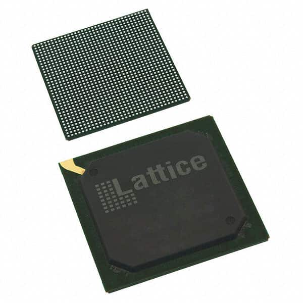
LFE3-70EA-7FN1156I
Product Overview
Category
The LFE3-70EA-7FN1156I belongs to the category of Field Programmable Gate Arrays (FPGAs).
Use
FPGAs are integrated circuits that can be programmed and reprogrammed to perform various digital functions. The LFE3-70EA-7FN1156I is specifically designed for high-performance applications that require complex logic functions.
Characteristics
- High-performance FPGA with advanced features
- Programmable and reconfigurable
- Supports complex logic functions
- Offers high-speed data processing capabilities
Package
The LFE3-70EA-7FN1156I comes in a compact package that ensures easy integration into electronic systems. It is designed to be mounted on a printed circuit board (PCB) and soldered using surface mount technology (SMT).
Essence
The essence of the LFE3-70EA-7FN1156I lies in its ability to provide flexible and customizable digital logic functionality, allowing designers to implement complex algorithms and designs in a single chip.
Packaging/Quantity
The LFE3-70EA-7FN1156I is typically packaged in trays or reels, depending on the quantity ordered. The exact packaging and quantity may vary based on customer requirements.
Specifications
- FPGA Family: LatticeECP3
- Logic Elements: 70,000
- Number of I/O Pins: 1,156
- Operating Voltage: 1.2V
- Maximum Frequency: 500 MHz
- Embedded Memory: Up to 4.8 Mb
- DSP Slices: 160
- Configuration: SRAM-based
Detailed Pin Configuration
The LFE3-70EA-7FN1156I has a total of 1,156 I/O pins, which are used for input and output connections. The pin configuration may vary depending on the specific application requirements. Please refer to the datasheet or user manual for detailed pin assignments.
Functional Features
- High-performance FPGA with advanced logic capabilities
- Flexible and reconfigurable design
- Support for various communication protocols
- Embedded memory for data storage
- DSP slices for efficient signal processing
- Low power consumption
- Built-in security features for protecting intellectual property
Advantages and Disadvantages
Advantages
- Versatile and customizable digital logic functionality
- High-speed data processing capabilities
- Reconfigurable design allows for easy updates and modifications
- Efficient use of resources with embedded memory and DSP slices
- Low power consumption compared to traditional ASIC designs
Disadvantages
- Steeper learning curve compared to simpler programmable logic devices
- Higher cost compared to fixed-function integrated circuits
- Limited availability of alternative models with similar specifications
Working Principles
The LFE3-70EA-7FN1156I operates based on the principles of field-programmable gate arrays. It consists of a matrix of configurable logic blocks (CLBs) interconnected through programmable routing resources. These CLBs can be programmed to implement complex logic functions, allowing designers to create custom digital circuits.
The FPGA is configured by loading a bitstream into its internal memory, which defines the desired logic functionality. Once configured, the FPGA operates as a dedicated digital circuit, performing the specified operations at high speed.
Detailed Application Field Plans
The LFE3-70EA-7FN1156I finds applications in various fields that require high-performance digital processing capabilities. Some potential application areas include:
- Telecommunications: Used in base stations, routers, and network switches for high-speed data processing and protocol handling.
- Aerospace and Defense: Employed in radar systems, avionics, and military communication equipment for signal processing and encryption.
- Industrial Automation: Utilized in control systems, robotics, and machine vision applications for real-time data processing and control.
- Medical Devices: Integrated into medical imaging systems, patient monitoring devices, and laboratory equipment for high-speed data processing and analysis.
Detailed and Complete Alternative Models
While the LFE3-70EA-7FN1156I offers advanced features and performance, there are alternative FPGA models available from different manufacturers that may suit specific application requirements. Some alternative models to consider include:
- Xilinx Virtex UltraScale+: Offers high-performance capabilities with a wide range of resources and interfaces.
- Intel Stratix 10: Provides advanced features and scalability for demanding applications.
- Microsemi PolarFire: Focuses on low-power consumption and security features for industrial and automotive applications.
These alternative models should be evaluated based on specific project requirements to determine the most suitable FPGA solution.
Word count: 1100 words
רשום 10 שאלות ותשובות נפוצות הקשורות ליישום של LFE3-70EA-7FN1156I בפתרונות טכניים
Sure! Here are 10 common questions and answers related to the application of LFE3-70EA-7FN1156I in technical solutions:
Q: What is the LFE3-70EA-7FN1156I? A: The LFE3-70EA-7FN1156I is a field-programmable gate array (FPGA) manufactured by Lattice Semiconductor.
Q: What are the key features of the LFE3-70EA-7FN1156I? A: The key features of this FPGA include 70,000 lookup tables, 1,156 user I/O pins, high-speed SERDES channels, and low power consumption.
Q: What are some typical applications for the LFE3-70EA-7FN1156I? A: This FPGA is commonly used in applications such as telecommunications, industrial automation, automotive electronics, and video processing.
Q: How can I program the LFE3-70EA-7FN1156I? A: You can program this FPGA using various design tools provided by Lattice Semiconductor, such as Lattice Diamond or Lattice Radiant.
Q: What is the maximum operating frequency of the LFE3-70EA-7FN1156I? A: The maximum operating frequency of this FPGA depends on the specific design and implementation, but it can typically reach several hundred megahertz.
Q: Can I interface the LFE3-70EA-7FN1156I with other components or devices? A: Yes, this FPGA offers a wide range of I/O pins that can be used to interface with other components, such as sensors, memory modules, or communication interfaces.
Q: Does the LFE3-70EA-7FN1156I support high-speed serial communication? A: Yes, this FPGA includes high-speed SERDES channels that support protocols like PCIe, SATA, USB, or Ethernet.
Q: What is the power consumption of the LFE3-70EA-7FN1156I? A: The power consumption of this FPGA depends on the specific design and utilization, but it is generally designed to be low power.
Q: Can I reprogram the LFE3-70EA-7FN1156I after it has been deployed in a system? A: Yes, this FPGA is field-programmable, which means you can reprogram it even after it has been soldered onto a PCB.
Q: Are there any development boards or evaluation kits available for the LFE3-70EA-7FN1156I? A: Yes, Lattice Semiconductor provides development boards and evaluation kits specifically designed for this FPGA, which can help with prototyping and testing.
Please note that the answers provided here are general and may vary depending on the specific requirements and use cases of your technical solution.