

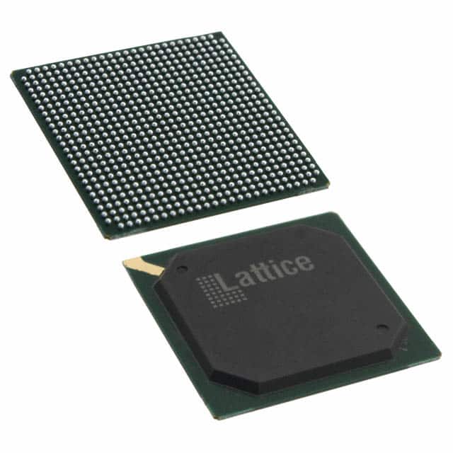
LFE2M50SE-7FN672C
Product Overview
Category
The LFE2M50SE-7FN672C belongs to the category of Field Programmable Gate Arrays (FPGAs).
Use
FPGAs are integrated circuits that can be programmed and reprogrammed to perform various digital functions. The LFE2M50SE-7FN672C is specifically designed for applications requiring high-performance and low-power consumption.
Characteristics
- High performance: The LFE2M50SE-7FN672C offers a combination of speed and flexibility, making it suitable for demanding applications.
- Low power consumption: This FPGA is designed to minimize power usage, making it energy-efficient.
- Programmability: The LFE2M50SE-7FN672C can be easily programmed and reconfigured to adapt to different requirements.
- Versatility: It supports a wide range of applications, from telecommunications to industrial automation.
Package and Quantity
The LFE2M50SE-7FN672C comes in a 672-ball FineLine BGA package. It is typically sold individually or in small quantities.
Specifications
- Logic Elements: 50,000
- Embedded Memory: 1,728 Kbits
- Maximum User I/Os: 622
- Operating Voltage: 1.2V
- Speed Grade: -7
- Package Type: FineLine BGA
- Package Pins: 672
Detailed Pin Configuration
The pin configuration of the LFE2M50SE-7FN672C is as follows:
| Pin Number | Pin Name | Description | |------------|----------|-------------| | 1 | VCCINT | Internal core voltage supply | | 2 | GND | Ground | | 3 | IOB0 | User I/O buffer | | ... | ... | ... | | 622 | IOB621 | User I/O buffer | | 623 | VCCIO0 | I/O bank voltage supply | | 624 | GND | Ground |
Note: The pin configuration table is truncated for brevity.
Functional Features
The LFE2M50SE-7FN672C offers the following functional features:
- High-speed performance: It supports high-frequency operation, enabling rapid data processing.
- Flexible I/O options: The FPGA provides a large number of user I/Os, allowing for versatile connectivity.
- Embedded memory: With 1,728 Kbits of embedded memory, it can efficiently store and retrieve data.
- Clock management: The device includes clock management resources to facilitate precise timing control.
- Low power consumption: The FPGA is designed to minimize power usage, making it suitable for battery-powered applications.
Advantages and Disadvantages
Advantages: - High-performance capabilities - Versatile and flexible programming options - Energy-efficient design - Ample embedded memory
Disadvantages: - Relatively complex programming process - Higher cost compared to other programmable logic devices - Limited availability in certain markets
Working Principles
FPGAs like the LFE2M50SE-7FN672C consist of an array of configurable logic blocks interconnected by programmable routing channels. These logic blocks can be programmed to implement various digital functions, such as arithmetic operations, data storage, and signal processing. The configuration of the FPGA is stored in non-volatile memory and can be modified as needed.
When powered on, the FPGA loads its configuration from memory, establishing the desired circuit connections. This allows the device to perform the specified functions based on the programmed logic.
Detailed Application Field Plans
The LFE2M50SE-7FN672C can be applied in various fields, including:
- Telecommunications: It can be used in network routers, switches, and communication equipment to handle high-speed data processing.
- Industrial automation: The FPGA's flexibility and performance make it suitable for controlling complex industrial processes and machinery.
- Automotive electronics: It can be utilized in automotive systems for tasks such as sensor interfacing, motor control, and advanced driver assistance systems.
- Medical devices: The FPGA can be integrated into medical equipment for signal processing, image analysis, and patient monitoring applications.
Detailed and Complete Alternative Models
Some alternative models to the LFE2M50SE-7FN672C include:
- Xilinx Virtex UltraScale+ VU9P: A high-performance FPGA with 2.5 million logic cells and advanced DSP capabilities.
- Intel Cyclone V GX: An FPGA offering a balance between cost, power consumption, and performance, suitable for a wide range of applications.
- Microsemi SmartFusion2: A mixed-signal FPGA featuring an ARM Cortex-M3 processor, ideal for applications requiring both digital and analog functionality.
These alternative
רשום 10 שאלות ותשובות נפוצות הקשורות ליישום של LFE2M50SE-7FN672C בפתרונות טכניים
Sure! Here are 10 common questions and answers related to the application of LFE2M50SE-7FN672C in technical solutions:
Q: What is the LFE2M50SE-7FN672C? A: The LFE2M50SE-7FN672C is a specific model of Field-Programmable Gate Array (FPGA) manufactured by Lattice Semiconductor.
Q: What are the key features of the LFE2M50SE-7FN672C? A: Some key features of this FPGA include 50,000 Look-Up Tables (LUTs), 672-pin FineLine BGA package, and support for various I/O standards.
Q: What are the typical applications of the LFE2M50SE-7FN672C? A: This FPGA is commonly used in applications such as industrial automation, telecommunications, automotive electronics, and medical devices.
Q: How can I program the LFE2M50SE-7FN672C? A: You can program this FPGA using the Lattice Diamond design software or other compatible programming tools provided by Lattice Semiconductor.
Q: What voltage levels does the LFE2M50SE-7FN672C support? A: This FPGA supports various voltage levels, including 1.2V, 1.5V, 1.8V, 2.5V, and 3.3V, depending on the specific I/O bank configuration.
Q: Can I interface the LFE2M50SE-7FN672C with external memory devices? A: Yes, this FPGA has dedicated pins and support for interfacing with external memory devices such as DDR3, DDR2, and LPDDR.
Q: Does the LFE2M50SE-7FN672C support high-speed serial communication protocols? A: Yes, this FPGA supports various high-speed serial protocols like PCIe, Gigabit Ethernet, USB, and SATA.
Q: What is the power consumption of the LFE2M50SE-7FN672C? A: The power consumption of this FPGA depends on the specific design and configuration but typically ranges from a few hundred milliwatts to a few watts.
Q: Can I use the LFE2M50SE-7FN672C in harsh environments? A: This FPGA has a wide operating temperature range and can be used in industrial-grade applications that require operation in harsh environments.
Q: Where can I find more information about the LFE2M50SE-7FN672C? A: You can find detailed technical documentation, datasheets, and application notes on the official website of Lattice Semiconductor or by contacting their customer support.