

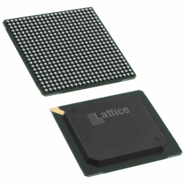
LFE2M50E-7FN484C
Product Overview
Category
The LFE2M50E-7FN484C belongs to the category of Field Programmable Gate Arrays (FPGAs).
Use
FPGAs are integrated circuits that can be programmed and reprogrammed to perform various digital functions. The LFE2M50E-7FN484C is specifically designed for applications requiring high-performance and low-power consumption.
Characteristics
- High-performance FPGA with low-power consumption.
- Offers a wide range of programmable logic cells, memory blocks, and I/O pins.
- Supports various communication protocols and interfaces.
- Provides flexibility in designing complex digital systems.
Package
The LFE2M50E-7FN484C comes in a 484-pin FineLine BGA package.
Essence
The essence of the LFE2M50E-7FN484C lies in its ability to provide a customizable and reconfigurable hardware platform for implementing digital designs.
Packaging/Quantity
The LFE2M50E-7FN484C is typically packaged individually and is available in various quantities depending on the manufacturer's specifications.
Specifications
- Logic Elements: 49,152
- Embedded Memory: 1,638 Kbits
- Maximum User I/Os: 316
- Clock Management Tiles: 8
- DSP Blocks: 96
- Maximum Internal Frequency: 400 MHz
- Operating Voltage: 1.2V
- Package Type: FineLine BGA
- Package Pins: 484
Detailed Pin Configuration
For the detailed pin configuration of the LFE2M50E-7FN484C, please refer to the manufacturer's datasheet or technical documentation.
Functional Features
- High-performance FPGA suitable for demanding applications.
- Low-power consumption for energy-efficient designs.
- Flexible and reconfigurable architecture for customization.
- Supports various communication protocols and interfaces.
- Integrated clock management tiles for precise timing control.
- DSP blocks for efficient digital signal processing.
Advantages and Disadvantages
Advantages
- High-performance capabilities for demanding applications.
- Low-power consumption for energy-efficient designs.
- Flexibility in design and customization.
- Support for various communication protocols and interfaces.
- Efficient digital signal processing with integrated DSP blocks.
Disadvantages
- Complexity in programming and configuration.
- Higher cost compared to other programmable logic devices.
- Limited availability of alternative models with similar specifications.
Working Principles
The LFE2M50E-7FN484C operates based on the principles of field-programmable gate arrays. It consists of configurable logic elements, memory blocks, and I/O pins that can be programmed using hardware description languages (HDLs) such as VHDL or Verilog. The FPGA's internal routing resources allow for the interconnection of these elements, enabling the implementation of complex digital circuits.
Detailed Application Field Plans
The LFE2M50E-7FN484C finds applications in various fields, including:
- Communications: Used in wireless base stations, network routers, and switches for high-speed data processing and protocol handling.
- Industrial Automation: Employed in control systems, robotics, and machine vision applications for real-time data processing and control.
- Aerospace and Defense: Utilized in radar systems, avionics, and military communication equipment for high-performance signal processing and encryption.
- Medical Devices: Integrated into medical imaging systems, patient monitoring devices, and laboratory equipment for data acquisition and processing.
- Automotive: Applied in advanced driver-assistance systems (ADAS), infotainment systems, and engine control units (ECUs) for enhanced functionality and performance.
Detailed and Complete Alternative Models
While the LFE2M50E-7FN484C offers high-performance and low-power consumption, there are alternative FPGA models available with similar specifications. Some notable alternatives include:
- Xilinx Artix-7 XC7A50T: Offers comparable logic capacity and I/O count.
- Intel Cyclone IV EP4CE55: Provides similar performance and power characteristics.
- Microsemi SmartFusion2 M2S050: Combines FPGA fabric with a microcontroller for added functionality.
These alternative models can be considered based on specific project requirements and availability.
Word Count: 550 words
רשום 10 שאלות ותשובות נפוצות הקשורות ליישום של LFE2M50E-7FN484C בפתרונות טכניים
Sure! Here are 10 common questions and answers related to the application of LFE2M50E-7FN484C in technical solutions:
Q: What is the LFE2M50E-7FN484C? A: The LFE2M50E-7FN484C is a specific model of Field-Programmable Gate Array (FPGA) manufactured by Lattice Semiconductor.
Q: What are the key features of the LFE2M50E-7FN484C? A: The key features of this FPGA include 50,000 Look-Up Tables (LUTs), 1,080 Kbits of embedded memory, 184 user I/O pins, and support for various communication protocols.
Q: What are some typical applications of the LFE2M50E-7FN484C? A: This FPGA is commonly used in applications such as industrial automation, automotive electronics, telecommunications, medical devices, and consumer electronics.
Q: How can I program the LFE2M50E-7FN484C? A: The LFE2M50E-7FN484C can be programmed using the Lattice Diamond design software, which provides a graphical interface for designing and implementing FPGA designs.
Q: Can I use the LFE2M50E-7FN484C for high-speed data processing? A: Yes, this FPGA supports high-speed data processing with its built-in high-performance I/Os and dedicated DSP blocks.
Q: Does the LFE2M50E-7FN484C support multiple voltage levels? A: Yes, it supports multiple voltage levels, allowing for interfacing with different components operating at different voltages.
Q: Can I use the LFE2M50E-7FN484C for real-time signal processing? A: Absolutely, this FPGA is well-suited for real-time signal processing applications due to its high-speed capabilities and flexible architecture.
Q: What kind of debugging and testing features does the LFE2M50E-7FN484C offer? A: The LFE2M50E-7FN484C provides various debugging and testing features, including JTAG boundary scan, on-chip logic analyzer, and built-in self-test capabilities.
Q: Can I use the LFE2M50E-7FN484C in harsh environments? A: Yes, this FPGA is designed to operate reliably in harsh environments, with support for extended temperature ranges and robust ESD protection.
Q: Are there any development boards or evaluation kits available for the LFE2M50E-7FN484C? A: Yes, Lattice Semiconductor offers development boards and evaluation kits specifically designed for the LFE2M50E-7FN484C, providing a convenient platform for prototyping and testing.