

LFE2M100E-6FN1152I
Product Overview
Category
The LFE2M100E-6FN1152I belongs to the category of Field Programmable Gate Arrays (FPGAs).
Use
This product is primarily used in digital logic circuits for various applications such as telecommunications, automotive, industrial automation, and consumer electronics.
Characteristics
- High-performance FPGA with advanced features
- Low power consumption
- Flexible and reconfigurable design
- High-speed data processing capabilities
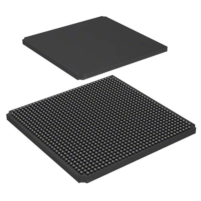
Package
The LFE2M100E-6FN1152I comes in a compact and durable package suitable for surface mount technology (SMT) assembly.
Essence
The essence of this FPGA lies in its ability to provide a customizable hardware platform that can be programmed to perform specific functions according to the user's requirements.
Packaging/Quantity
The LFE2M100E-6FN1152I is typically packaged in reels or trays, containing a specific quantity of units per package. The exact packaging and quantity may vary depending on the manufacturer.
Specifications
- FPGA Family: Lattice ECP2M
- Logic Elements: 100,000
- Number of I/O Pins: 1,152
- Operating Voltage: 1.2V
- Maximum Frequency: 300 MHz
- Embedded Memory: Up to 4.8 Mbits
- Configuration Memory: On-chip Flash memory
Detailed Pin Configuration
The LFE2M100E-6FN1152I has a total of 1,152 I/O pins, which are configurable based on the desired functionality. The pin configuration can be found in the product datasheet provided by the manufacturer.
Functional Features
- High-speed serial transceivers for high-bandwidth data communication
- Dedicated DSP blocks for efficient signal processing
- Flexible clock management resources
- On-chip memory blocks for data storage and retrieval
- Built-in security features to protect intellectual property
Advantages and Disadvantages
Advantages
- Versatile and customizable design
- Low power consumption
- High-performance capabilities
- Suitable for a wide range of applications
- Cost-effective solution compared to custom ASIC designs
Disadvantages
- Steep learning curve for beginners
- Limited availability of technical support compared to mainstream FPGAs
- Higher cost compared to general-purpose microcontrollers
Working Principles
The LFE2M100E-6FN1152I operates based on the principles of reconfigurable logic. It consists of an array of programmable logic elements interconnected through configurable routing resources. The user can program the FPGA using hardware description languages (HDLs) such as VHDL or Verilog to define the desired functionality.
Detailed Application Field Plans
The LFE2M100E-6FN1152I can be applied in various fields, including:
- Telecommunications: Used in base stations, routers, and network switches for high-speed data processing and communication.
- Automotive: Employed in automotive control systems, infotainment systems, and driver assistance systems.
- Industrial Automation: Utilized in industrial control systems, robotics, and machine vision applications.
- Consumer Electronics: Integrated into multimedia devices, gaming consoles, and smart home appliances.
Detailed and Complete Alternative Models
- Xilinx Virtex UltraScale+ FPGA
- Intel Stratix 10 FPGA
- Microsemi PolarFire FPGA
- QuickLogic EOS S3 FPGA
- Actel Fusion FPGA
These alternative models offer similar functionalities and can be considered as alternatives to the LFE2M100E-6FN1152I depending on specific requirements.
Word count: 530 words
רשום 10 שאלות ותשובות נפוצות הקשורות ליישום של LFE2M100E-6FN1152I בפתרונות טכניים
Sure! Here are 10 common questions and answers related to the application of LFE2M100E-6FN1152I in technical solutions:
Q: What is the LFE2M100E-6FN1152I? A: The LFE2M100E-6FN1152I is a specific model of Field-Programmable Gate Array (FPGA) manufactured by Lattice Semiconductor.
Q: What are the key features of the LFE2M100E-6FN1152I? A: The key features of this FPGA include 100,000 logic elements, low power consumption, high-speed performance, and support for various I/O standards.
Q: What are some typical applications of the LFE2M100E-6FN1152I? A: This FPGA is commonly used in applications such as industrial automation, telecommunications, automotive electronics, medical devices, and video processing.
Q: How can I program the LFE2M100E-6FN1152I? A: The LFE2M100E-6FN1152I can be programmed using industry-standard hardware description languages (HDLs) like VHDL or Verilog, along with appropriate development tools provided by Lattice Semiconductor.
Q: What are the voltage requirements for the LFE2M100E-6FN1152I? A: The LFE2M100E-6FN1152I operates at a core voltage of 1.2V and supports various I/O voltage standards, including 1.8V, 2.5V, and 3.3V.
Q: Can I use the LFE2M100E-6FN1152I in a high-reliability application? A: Yes, the LFE2M100E-6FN1152I is designed to meet the requirements of high-reliability applications and is suitable for use in harsh environments.
Q: Does the LFE2M100E-6FN1152I support external memory interfaces? A: Yes, this FPGA supports various external memory interfaces such as DDR3, DDR4, and LPDDR4, allowing for efficient data storage and retrieval.
Q: Can I interface the LFE2M100E-6FN1152I with other devices or microcontrollers? A: Absolutely! The LFE2M100E-6FN1152I provides a range of I/O options, including LVCMOS, LVDS, and differential signaling, making it compatible with various devices and microcontrollers.
Q: What kind of development tools are available for programming and debugging the LFE2M100E-6FN1152I? A: Lattice Semiconductor provides a comprehensive suite of development tools, including the Lattice Diamond design software, which offers synthesis, simulation, and debugging capabilities.
Q: Where can I find additional technical documentation and support for the LFE2M100E-6FN1152I? A: You can visit the official website of Lattice Semiconductor to access datasheets, application notes, user guides, and technical support resources for the LFE2M100E-6FN1152I FPGA.