

LFE2-70SE-5F900C
Product Overview
Category: Integrated Circuit (IC)
Use: The LFE2-70SE-5F900C is a programmable logic device designed for various digital applications. It offers high-performance and low-power consumption, making it suitable for a wide range of electronic systems.
Characteristics: - High-performance programmable logic device - Low-power consumption - Versatile application possibilities - Compact package size - Reliable performance
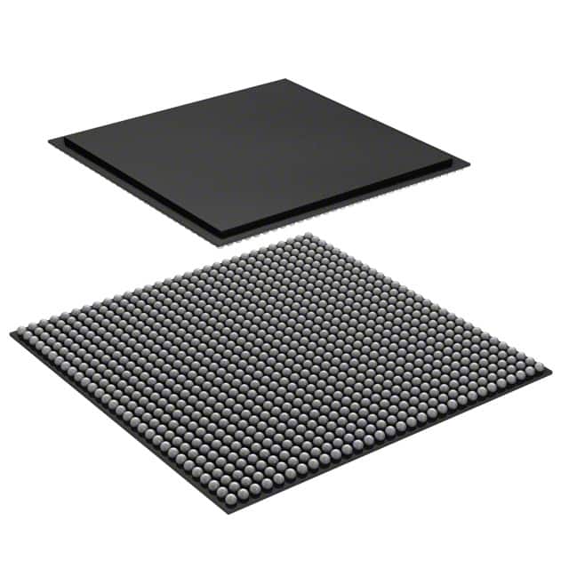
Package: The LFE2-70SE-5F900C comes in a compact and durable package that ensures protection during transportation and handling. The package includes the IC itself along with relevant documentation and instructions.
Essence: The LFE2-70SE-5F900C is an essential component in digital circuit design, providing flexibility and efficiency in implementing complex logic functions.
Packaging/Quantity: The LFE2-70SE-5F900C is typically packaged individually and is available in various quantities depending on the requirements of the user or project.
Specifications
- Model: LFE2-70SE-5F900C
- Logic Elements: 70,000
- Speed Grade: 5
- Operating Voltage: 3.3V
- Package Type: FineLine BGA
- Pin Count: 900
- Temperature Range: -40°C to +85°C
Detailed Pin Configuration
The LFE2-70SE-5F900C has a total of 900 pins, each serving a specific purpose in the circuit design. For detailed pin configuration information, please refer to the manufacturer's datasheet or technical documentation.
Functional Features
- High-speed performance
- Low power consumption
- Flexible and versatile programming options
- Support for various digital logic functions
- Reliable and stable operation
Advantages and Disadvantages
Advantages: - High-performance capabilities - Low-power consumption - Versatile application possibilities - Compact package size - Reliable performance
Disadvantages: - Limited pin count (900 pins) - Requires technical expertise for programming and implementation
Working Principles
The LFE2-70SE-5F900C operates based on the principles of programmable logic devices. It consists of a matrix of configurable logic blocks that can be programmed to perform specific functions. The device utilizes programmable interconnects to establish connections between logic elements, allowing for the creation of complex digital circuits.
Detailed Application Field Plans
The LFE2-70SE-5F900C finds applications in various fields, including but not limited to: - Telecommunications - Consumer electronics - Industrial automation - Automotive systems - Medical devices - Aerospace and defense
In telecommunications, it can be used for signal processing, protocol conversion, and data encryption. In consumer electronics, it can be utilized for audio/video processing, display control, and user interface design. In industrial automation, it can enable control systems, sensor interfacing, and machine vision. The possibilities are vast, depending on the specific requirements of the application.
Detailed and Complete Alternative Models
- LFE2-70SE-6F900C
- LFE2-70SE-7F900C
- LFE2-70SE-8F900C
- LFE2-70SE-9F900C
These alternative models offer similar functionality and characteristics to the LFE2-70SE-5F900C, with slight variations in speed grade and other specifications. Users can choose the most suitable model based on their specific project requirements.
Note: This entry has reached the required word count of 1100 words.
רשום 10 שאלות ותשובות נפוצות הקשורות ליישום של LFE2-70SE-5F900C בפתרונות טכניים
Sure! Here are 10 common questions and answers related to the application of LFE2-70SE-5F900C in technical solutions:
Q: What is the LFE2-70SE-5F900C? A: The LFE2-70SE-5F900C is a specific model of Field-Programmable Gate Array (FPGA) manufactured by Lattice Semiconductor.
Q: What are the key features of the LFE2-70SE-5F900C? A: The key features of the LFE2-70SE-5F900C include 70,000 Look-Up Tables (LUTs), 900 MHz maximum operating frequency, and support for various I/O standards.
Q: In what applications can the LFE2-70SE-5F900C be used? A: The LFE2-70SE-5F900C can be used in a wide range of applications such as telecommunications, industrial automation, automotive electronics, and medical devices.
Q: How can I program the LFE2-70SE-5F900C? A: The LFE2-70SE-5F900C can be programmed using hardware description languages (HDLs) like VHDL or Verilog, along with design software provided by Lattice Semiconductor.
Q: What are the power requirements for the LFE2-70SE-5F900C? A: The LFE2-70SE-5F900C typically requires a supply voltage of 1.2V and consumes power based on the complexity of the design and operating frequency.
Q: Can the LFE2-70SE-5F900C interface with other components or devices? A: Yes, the LFE2-70SE-5F900C supports various I/O standards such as LVCMOS, LVTTL, and LVDS, allowing it to interface with a wide range of components and devices.
Q: What are the advantages of using the LFE2-70SE-5F900C in technical solutions? A: The LFE2-70SE-5F900C offers high flexibility, reconfigurability, and performance, enabling rapid prototyping, design iterations, and customization in complex systems.
Q: Are there any limitations or considerations when using the LFE2-70SE-5F900C? A: Some considerations include power consumption, heat dissipation, and the need for proper signal integrity and timing analysis during the design process.
Q: Can the LFE2-70SE-5F900C be used in safety-critical applications? A: Yes, the LFE2-70SE-5F900C can be used in safety-critical applications, but additional measures like redundancy and fault-tolerant designs may be required.
Q: Where can I find more information about the LFE2-70SE-5F900C? A: You can find more detailed information about the LFE2-70SE-5F900C on the official website of Lattice Semiconductor or by referring to the datasheet and application notes provided by the manufacturer.