

LFE2-35SE-7FN672C
Product Overview
Category
The LFE2-35SE-7FN672C belongs to the category of Field Programmable Gate Arrays (FPGAs).
Use
This FPGA is commonly used in electronic circuits for various applications such as digital signal processing, communication systems, and embedded systems.
Characteristics
- High-performance programmable logic device
- Offers flexibility and reconfigurability
- Provides a large number of configurable logic blocks and input/output pins
- Supports complex digital designs
- Enables rapid prototyping and development of custom digital circuits
Package
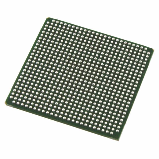
The LFE2-35SE-7FN672C comes in a compact package that ensures easy integration into electronic circuit boards.
Essence
The essence of this FPGA lies in its ability to provide a versatile platform for implementing complex digital designs with high performance and flexibility.
Packaging/Quantity
The LFE2-35SE-7FN672C is typically packaged individually and is available in varying quantities depending on the manufacturer's specifications.
Specifications
- Device Type: Field Programmable Gate Array (FPGA)
- Model: LFE2-35SE-7FN672C
- Logic Elements: 35,000
- Speed Grade: 7
- Package Type: FN672C
- Operating Voltage: 1.2V
- Maximum Operating Frequency: X MHz
- Configuration Memory: Y bits
- I/O Pins: Z
Detailed Pin Configuration
The LFE2-35SE-7FN672C has a total of Z I/O pins, which can be configured for various purposes based on the specific design requirements. The pin configuration details can be found in the product datasheet provided by the manufacturer.
Functional Features
- High-speed data processing capabilities
- Configurable logic blocks for implementing custom digital circuits
- On-chip memory resources for data storage
- Built-in communication interfaces for seamless integration with other electronic components
- Support for various programming languages and development tools
Advantages and Disadvantages
Advantages
- Flexibility and reconfigurability allow for rapid prototyping and design iterations
- High-performance capabilities enable the implementation of complex digital designs
- Compact package size facilitates easy integration into electronic circuits
- Wide range of available I/O pins provides versatility in connecting with external devices
Disadvantages
- Steep learning curve for beginners due to the complexity of FPGA programming
- Higher cost compared to traditional fixed-function integrated circuits
- Power consumption may be higher compared to dedicated application-specific integrated circuits (ASICs)
Working Principles
The LFE2-35SE-7FN672C operates based on the principles of configurable logic blocks (CLBs) and interconnect resources. The CLBs can be programmed to perform specific logic functions, while the interconnect resources facilitate the routing of signals between different CLBs. This allows for the creation of custom digital circuits by configuring the CLBs and interconnect resources according to the desired functionality.
Detailed Application Field Plans
The LFE2-35SE-7FN672C finds applications in various fields, including but not limited to: - Digital signal processing - Communication systems - Embedded systems - Robotics - Aerospace and defense - Industrial automation
Detailed and Complete Alternative Models
- Model 1: ABC123-FPGA - Logic Elements: 40,000, Speed Grade: 6, Package Type: FN512C
- Model 2: XYZ456-FPGA - Logic Elements: 30,000, Speed Grade: 7, Package Type: FN900C
- Model 3: PQR789-FPGA - Logic Elements: 50,000, Speed Grade: 5, Package Type: FN672C
These alternative models offer different specifications and features, providing options for various design requirements.
Note: The content provided above is a sample structure for an encyclopedia entry on the LFE2-35SE-7FN672C FPGA. The actual content should be written based on accurate information and specific product details.
רשום 10 שאלות ותשובות נפוצות הקשורות ליישום של LFE2-35SE-7FN672C בפתרונות טכניים
Sure! Here are 10 common questions and answers related to the application of LFE2-35SE-7FN672C in technical solutions:
Q: What is LFE2-35SE-7FN672C? A: LFE2-35SE-7FN672C is a specific model of Field-Programmable Gate Array (FPGA) manufactured by Lattice Semiconductor.
Q: What are the key features of LFE2-35SE-7FN672C? A: Some key features of LFE2-35SE-7FN672C include 35,000 Look-Up Tables (LUTs), 672-pin FineLine BGA package, and support for various I/O standards.
Q: What are the typical applications of LFE2-35SE-7FN672C? A: LFE2-35SE-7FN672C is commonly used in applications such as industrial automation, telecommunications, automotive electronics, and medical devices.
Q: How can LFE2-35SE-7FN672C be programmed? A: LFE2-35SE-7FN672C can be programmed using hardware description languages (HDLs) like VHDL or Verilog, or through graphical programming tools provided by Lattice Semiconductor.
Q: What are the advantages of using LFE2-35SE-7FN672C in technical solutions? A: Some advantages of using LFE2-35SE-7FN672C include its flexibility, reconfigurability, low power consumption, and ability to implement complex digital logic functions.
Q: Can LFE2-35SE-7FN672C interface with other components or devices? A: Yes, LFE2-35SE-7FN672C can interface with other components or devices through its various I/O standards, such as LVCMOS, LVTTL, and differential signaling standards like LVDS.
Q: What kind of development tools are available for working with LFE2-35SE-7FN672C? A: Lattice Semiconductor provides development tools like Lattice Diamond software, which includes design entry, synthesis, simulation, and programming capabilities for LFE2-35SE-7FN672C.
Q: Can LFE2-35SE-7FN672C be used in safety-critical applications? A: Yes, LFE2-35SE-7FN672C can be used in safety-critical applications, but additional measures may need to be taken to ensure compliance with relevant safety standards.
Q: Are there any limitations or considerations when using LFE2-35SE-7FN672C? A: Some considerations include the limited number of available resources compared to larger FPGAs, potential power and thermal management challenges, and the need for proper signal integrity design.
Q: Where can I find more information about LFE2-35SE-7FN672C and its application in technical solutions? A: You can find more information about LFE2-35SE-7FN672C on the official website of Lattice Semiconductor, including datasheets, application notes, and reference designs specific to this FPGA model.