

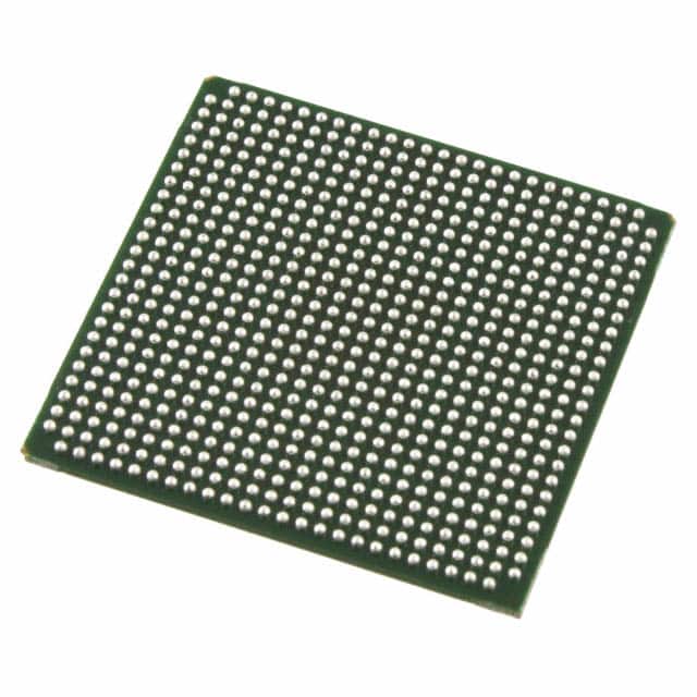
LFE2-35E-7FN672C
Product Overview
Category
The LFE2-35E-7FN672C belongs to the category of Field Programmable Gate Arrays (FPGAs).
Use
This FPGA is commonly used in electronic devices and systems for digital logic implementation, such as in telecommunications, automotive, aerospace, and consumer electronics.
Characteristics
- High-performance programmable logic device
- Offers flexibility and reconfigurability
- Allows for rapid prototyping and development of custom digital circuits
- Provides high-speed data processing capabilities
- Supports complex algorithms and computations
Package
The LFE2-35E-7FN672C comes in a compact and durable package, ensuring protection during handling and installation.
Essence
The essence of this FPGA lies in its ability to provide a versatile platform for implementing various digital logic designs, enabling efficient and customizable solutions for different applications.
Packaging/Quantity
The LFE2-35E-7FN672C is typically packaged individually and is available in varying quantities depending on the manufacturer or supplier.
Specifications
- Device Type: Field Programmable Gate Array (FPGA)
- Model: LFE2-35E-7FN672C
- Logic Elements: 35,000
- Number of I/O Pins: 672
- Operating Voltage: 1.2V
- Maximum Frequency: 500 MHz
- Configuration Memory: Flash-based
- Package Type: Fine-pitch Ball Grid Array (FBGA)
Detailed Pin Configuration
The LFE2-35E-7FN672C has a total of 672 pins, which are assigned to various functions such as input, output, power supply, and configuration. The pin configuration may vary depending on the specific application requirements and design considerations.
Functional Features
- High-density programmable logic elements for complex digital circuit implementation
- Dedicated high-speed I/O pins for efficient data transfer
- Embedded memory blocks for storing intermediate results and configuration data
- Flexible clock management resources for precise timing control
- Built-in digital signal processing (DSP) blocks for performing complex mathematical operations
- Support for various communication protocols and interfaces
Advantages and Disadvantages
Advantages
- Versatile and customizable solution for digital logic implementation
- Rapid prototyping and development capabilities
- High-performance and high-speed data processing
- Reconfigurable nature allows for design iterations and updates
- Supports complex algorithms and computations
Disadvantages
- Requires expertise in FPGA programming and design
- Higher cost compared to fixed-function integrated circuits
- Power consumption may be higher compared to dedicated hardware solutions
- Limited availability of alternative models with similar specifications
Working Principles
The LFE2-35E-7FN672C operates based on the principles of reconfigurable computing. It consists of an array of programmable logic elements interconnected through configurable routing resources. These logic elements can be programmed to implement desired digital functions, allowing for the creation of custom digital circuits.
The FPGA is configured by loading a bitstream into its configuration memory, which determines the functionality of each logic element and the interconnections between them. Once configured, the FPGA performs the desired digital operations based on the programmed logic.
Detailed Application Field Plans
The LFE2-35E-7FN672C finds applications in various fields, including:
- Telecommunications: Used in network infrastructure equipment for high-speed data processing, protocol conversion, and signal modulation/demodulation.
- Automotive: Employed in advanced driver-assistance systems (ADAS) for real-time image processing, sensor fusion, and control algorithms.
- Aerospace: Utilized in avionics systems for flight control, data acquisition, and communication interfaces.
- Consumer Electronics: Integrated into multimedia devices, gaming consoles, and high-definition displays for video processing, audio decoding, and user interface control.
Detailed and Complete Alternative Models
- LFE2-35E-6FN672C: Similar to the LFE2-35E-7FN672C but with a lower maximum frequency of 400 MHz.
- LFE2-35E-8FN672C: Similar to the LFE2-35E-7FN672C but with additional logic elements (40,000) and I/O pins (800).
- LFE2-35E-7FN484C: A variant with a smaller package size (484-pin Fine-pitch Ball Grid Array) while maintaining similar specifications.
These alternative models offer different trade-offs in terms of performance, pin count, and package size, allowing designers to choose the most suitable option for their specific requirements.
Word count: 615 words
רשום 10 שאלות ותשובות נפוצות הקשורות ליישום של LFE2-35E-7FN672C בפתרונות טכניים
Sure! Here are 10 common questions and answers related to the application of LFE2-35E-7FN672C in technical solutions:
Q: What is the LFE2-35E-7FN672C? A: The LFE2-35E-7FN672C is a specific model of Field-Programmable Gate Array (FPGA) manufactured by Lattice Semiconductor.
Q: What are the key features of the LFE2-35E-7FN672C? A: Some key features of this FPGA include 35,000 Look-Up Tables (LUTs), 672-pin FineLine BGA package, low power consumption, and high-speed performance.
Q: In what applications can the LFE2-35E-7FN672C be used? A: This FPGA can be used in various applications such as industrial automation, telecommunications, automotive electronics, medical devices, and consumer electronics.
Q: How does the LFE2-35E-7FN672C contribute to industrial automation? A: It enables the implementation of complex control algorithms, real-time monitoring, and communication interfaces required for industrial automation systems.
Q: Can the LFE2-35E-7FN672C be used in telecommunications equipment? A: Yes, it can be used in telecommunications equipment for tasks like signal processing, protocol conversion, and network interface implementation.
Q: What advantages does the LFE2-35E-7FN672C offer in automotive electronics? A: It provides flexibility for implementing advanced driver assistance systems, infotainment systems, and vehicle control units with high reliability and performance.
Q: How does the LFE2-35E-7FN672C support medical devices? A: It enables the development of medical devices with advanced imaging capabilities, signal processing algorithms, and connectivity options.
Q: Can the LFE2-35E-7FN672C be used in consumer electronics? A: Yes, it can be used in consumer electronics for applications like video and audio processing, image recognition, and user interface implementation.
Q: What are the power requirements for the LFE2-35E-7FN672C? A: The power consumption of this FPGA is relatively low, typically operating at around 1.2V to 3.3V.
Q: How can I program the LFE2-35E-7FN672C? A: You can program this FPGA using various design tools provided by Lattice Semiconductor, such as Lattice Diamond or Lattice Radiant software.
Please note that the specific details and answers may vary depending on the context and requirements of your technical solution.