

LCMXO3LF-6900C-5BG400I
Product Overview
Category: Programmable Logic Device (PLD)
Use: The LCMXO3LF-6900C-5BG400I is a high-performance PLD designed for various digital logic applications. It offers flexibility and versatility in implementing complex digital circuits.
Characteristics: - Low power consumption - High-speed performance - Small form factor - Easy programmability - Wide range of I/O options
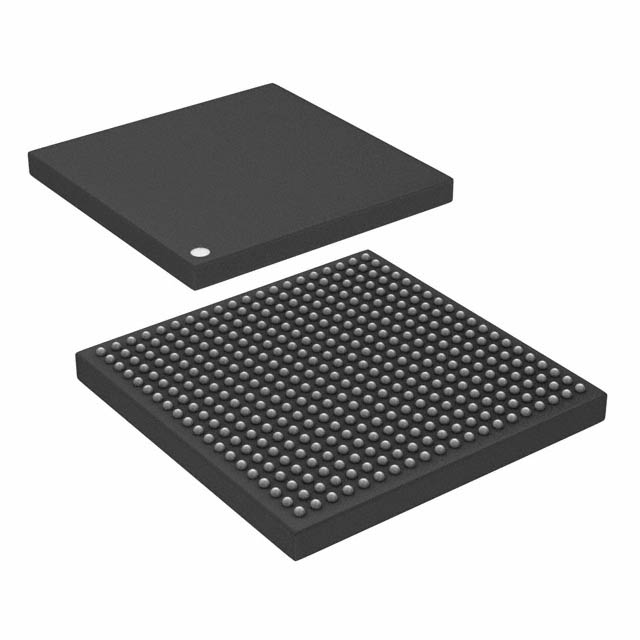
Package: The LCMXO3LF-6900C-5BG400I comes in a compact BGA (Ball Grid Array) package, which provides excellent thermal dissipation and mechanical stability.
Essence: This PLD is built to provide efficient and reliable digital logic implementation, enabling designers to create custom circuits tailored to their specific requirements.
Packaging/Quantity: The LCMXO3LF-6900C-5BG400I is typically sold individually or in small quantities, depending on the supplier.
Specifications
- Logic Cells: 6,900
- I/O Pins: 400
- Block RAM: 5,000 Kbits
- Clock Management Tiles: 8
- Maximum Frequency: 300 MHz
- Operating Voltage: 1.2V
- Package Type: BGA
- Temperature Range: -40°C to +85°C
Detailed Pin Configuration
The LCMXO3LF-6900C-5BG400I has a well-defined pin configuration that facilitates easy integration into circuit designs. The detailed pinout can be found in the product datasheet.
Functional Features
- Programmable logic cells allow for flexible circuit design and implementation.
- Dedicated clock management tiles enable precise timing control.
- Abundant I/O pins provide connectivity options for interfacing with external devices.
- Block RAM resources offer on-chip memory for data storage and processing.
Advantages and Disadvantages
Advantages: - Low power consumption makes it suitable for battery-powered applications. - High-speed performance enables efficient execution of complex logic operations. - Small form factor saves board space and simplifies system integration. - Easy programmability allows for quick prototyping and design iterations. - Wide range of I/O options facilitates versatile connectivity.
Disadvantages: - Limited logic cell count may restrict the complexity of designs. - BGA package requires specialized equipment for soldering and rework. - Higher cost compared to simpler PLDs or microcontrollers.
Working Principles
The LCMXO3LF-6900C-5BG400I operates based on the principles of field-programmable gate arrays (FPGAs). It consists of an array of configurable logic cells interconnected through programmable routing resources. The device can be programmed using hardware description languages (HDLs) or graphical tools, allowing designers to define the desired digital circuit functionality.
Detailed Application Field Plans
The LCMXO3LF-6900C-5BG400I finds applications in various fields, including: 1. Industrial automation 2. Communications systems 3. Consumer electronics 4. Automotive electronics 5. Medical devices
In industrial automation, it can be used for control systems, motor drives, and sensor interfacing. In communications systems, it enables protocol handling, signal processing, and network interfaces. In consumer electronics, it supports audio/video processing, user interface control, and connectivity features. In automotive electronics, it aids in vehicle control, driver assistance systems, and infotainment. In medical devices, it assists in imaging systems, patient monitoring, and diagnostic equipment.
Detailed and Complete Alternative Models
- LCMXO2LF-256HC-4SG32C
- LCMXO3LF-6900C-6BG400I
- LCMXO4LF-1200E-5BG256C
These alternative models offer similar functionality and performance but may vary in terms of logic cell count, I/O pins, package type, or other specifications. Designers can choose the most suitable model based on their specific requirements.
Note: The content provided above is a general outline for an encyclopedia entry on the LCMXO3LF-6900C-5BG400I. Additional information and details can be added as per the specific requirements and guidelines.
רשום 10 שאלות ותשובות נפוצות הקשורות ליישום של LCMXO3LF-6900C-5BG400I בפתרונות טכניים
Sure! Here are 10 common questions and answers related to the application of LCMXO3LF-6900C-5BG400I in technical solutions:
Q: What is the LCMXO3LF-6900C-5BG400I? A: The LCMXO3LF-6900C-5BG400I is a specific model of Field-Programmable Gate Array (FPGA) manufactured by Lattice Semiconductor.
Q: What are the key features of the LCMXO3LF-6900C-5BG400I? A: Some key features include low power consumption, small form factor, high-performance logic fabric, and embedded memory blocks.
Q: What are the typical applications of the LCMXO3LF-6900C-5BG400I? A: The LCMXO3LF-6900C-5BG400I is commonly used in various technical solutions such as industrial automation, consumer electronics, telecommunications, and automotive systems.
Q: How can I program the LCMXO3LF-6900C-5BG400I? A: The LCMXO3LF-6900C-5BG400I can be programmed using industry-standard hardware description languages (HDLs) like VHDL or Verilog.
Q: What tools are available for designing with the LCMXO3LF-6900C-5BG400I? A: Lattice Semiconductor provides software tools like Lattice Diamond or Lattice Radiant, which offer design entry, synthesis, simulation, and programming capabilities.
Q: Can the LCMXO3LF-6900C-5BG400I be reprogrammed after deployment? A: Yes, the LCMXO3LF-6900C-5BG400I is a reprogrammable FPGA, allowing for updates and modifications to the design even after deployment.
Q: What are the power requirements for the LCMXO3LF-6900C-5BG400I? A: The LCMXO3LF-6900C-5BG400I operates at low power, typically requiring a supply voltage of 1.2V or 3.3V.
Q: Can the LCMXO3LF-6900C-5BG400I interface with other components or devices? A: Yes, the LCMXO3LF-6900C-5BG400I supports various communication interfaces like SPI, I2C, UART, and GPIOs, enabling seamless integration with other components or devices.
Q: Are there any development boards available for prototyping with the LCMXO3LF-6900C-5BG400I? A: Yes, Lattice Semiconductor offers development boards like the LCMXO3L-6900C-B-EVN, which provide a platform for rapid prototyping and evaluation.
Q: Where can I find additional technical documentation and support for the LCMXO3LF-6900C-5BG400I? A: You can find detailed datasheets, application notes, reference designs, and support resources on the official website of Lattice Semiconductor or by contacting their technical support team.