

LCMXO2-1200ZE-3MG132IR1
Product Overview
Category
The LCMXO2-1200ZE-3MG132IR1 belongs to the category of Field-Programmable Gate Arrays (FPGAs).
Use
This FPGA is commonly used in electronic design and prototyping applications, where it provides a flexible and customizable digital logic solution.
Characteristics
- Low power consumption
- Small form factor
- High performance
- Easy programmability
Package
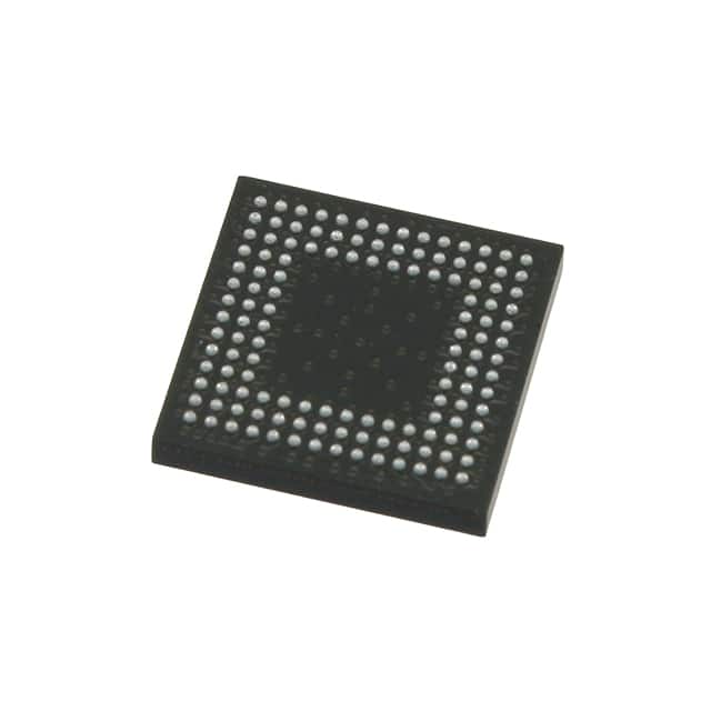
The LCMXO2-1200ZE-3MG132IR1 comes in a compact package that measures 13x13 mm.
Essence
The essence of this FPGA lies in its ability to be programmed and reprogrammed to perform various digital logic functions, making it highly versatile for different applications.
Packaging/Quantity
The LCMXO2-1200ZE-3MG132IR1 is typically packaged individually and is available in various quantities depending on the manufacturer or distributor.
Specifications
- Model: LCMXO2-1200ZE-3MG132IR1
- Logic Elements: 1200
- Macrocells: 132
- Speed Grade: 3
- Operating Voltage: 1.2V
- I/O Pins: 132
- Maximum Frequency: 100 MHz
- Configuration Memory: 64 Kbits
- Package Type: QFN
Detailed Pin Configuration
The LCMXO2-1200ZE-3MG132IR1 has a total of 132 I/O pins, each serving a specific purpose in the circuit design. The pin configuration can be found in the product datasheet provided by the manufacturer.
Functional Features
- Programmable logic elements for custom digital circuit implementation.
- Dedicated memory blocks for storing configuration data.
- Built-in I/O pins for interfacing with external devices.
- Clock management resources for precise timing control.
- On-chip power supply and voltage regulators for efficient operation.
Advantages and Disadvantages
Advantages
- Flexibility: The FPGA can be reprogrammed to adapt to changing design requirements.
- Customizability: Allows designers to create unique digital logic circuits tailored to their specific needs.
- Prototyping: Enables rapid prototyping and testing of complex digital systems.
- High Performance: Capable of handling demanding computational tasks.
Disadvantages
- Complexity: Designing and programming FPGAs requires specialized knowledge and expertise.
- Cost: FPGAs can be more expensive compared to other integrated circuits.
- Power Consumption: Depending on the design, FPGAs may consume more power than dedicated ASICs.
Working Principles
The LCMXO2-1200ZE-3MG132IR1 operates based on the principles of configurable logic. It consists of a matrix of programmable logic elements interconnected by configurable routing resources. These logic elements can be programmed to implement various digital functions, such as arithmetic operations, memory storage, and control logic. The configuration data is stored in on-chip memory blocks and can be modified using specialized software tools.
Detailed Application Field Plans
The LCMXO2-1200ZE-3MG132IR1 finds applications in a wide range of fields, including:
- Embedded Systems: Used for implementing custom digital interfaces and control systems in embedded devices.
- Communications: Employed in networking equipment for protocol processing and data manipulation.
- Industrial Automation: Utilized in automation systems for controlling machinery and monitoring processes.
- Consumer Electronics: Integrated into consumer devices for signal processing and user interface control.
- Automotive: Used in automotive electronics for engine control, driver assistance systems, and infotainment.
Detailed and Complete Alternative Models
- LCMXO2-640HC-4SG32C: A lower-capacity FPGA with 640 logic elements and 32 I/O pins.
- LCMXO3LF-6900C-5BG256C: A higher-capacity FPGA with 6900 logic elements and 256 I/O pins.
- LCMXO2-1200ZE-1TG144I: A variant of the LCMXO2-1200ZE series with a different package type.
These alternative models offer different capacities, pin counts, and package options to suit specific design requirements.
Word count: 524 words
רשום 10 שאלות ותשובות נפוצות הקשורות ליישום של LCMXO2-1200ZE-3MG132IR1 בפתרונות טכניים
Sure! Here are 10 common questions and answers related to the application of LCMXO2-1200ZE-3MG132IR1 in technical solutions:
Q1: What is the LCMXO2-1200ZE-3MG132IR1? A1: The LCMXO2-1200ZE-3MG132IR1 is a low-cost, low-power FPGA (Field-Programmable Gate Array) device manufactured by Lattice Semiconductor.
Q2: What are the key features of LCMXO2-1200ZE-3MG132IR1? A2: Some key features of LCMXO2-1200ZE-3MG132IR1 include 1200 Look-Up Tables (LUTs), 64 Kbits of embedded block RAM, 49 user I/O pins, and support for various I/O standards.
Q3: What are the typical applications of LCMXO2-1200ZE-3MG132IR1? A3: LCMXO2-1200ZE-3MG132IR1 is commonly used in applications such as industrial automation, consumer electronics, communication systems, and automotive electronics.
Q4: How can I program the LCMXO2-1200ZE-3MG132IR1? A4: The LCMXO2-1200ZE-3MG132IR1 can be programmed using Lattice Diamond or Lattice Radiant software tools, which provide a graphical interface for designing and programming the FPGA.
Q5: What voltage levels does LCMXO2-1200ZE-3MG132IR1 support? A5: LCMXO2-1200ZE-3MG132IR1 supports both 3.3V and 1.2V voltage levels, making it compatible with a wide range of devices and systems.
Q6: Can I use LCMXO2-1200ZE-3MG132IR1 in battery-powered applications? A6: Yes, LCMXO2-1200ZE-3MG132IR1 is designed to be low-power, making it suitable for battery-powered applications where power consumption is a concern.
Q7: Does LCMXO2-1200ZE-3MG132IR1 support communication protocols like UART or SPI? A7: Yes, LCMXO2-1200ZE-3MG132IR1 supports various communication protocols, including UART, SPI, I2C, and GPIO, allowing for easy integration with other devices.
Q8: Can I use LCMXO2-1200ZE-3MG132IR1 for real-time signal processing? A8: Yes, LCMXO2-1200ZE-3MG132IR1 can be used for real-time signal processing tasks due to its high-speed performance and flexible programmability.
Q9: Are there any development boards available for LCMXO2-1200ZE-3MG132IR1? A9: Yes, Lattice Semiconductor offers development boards specifically designed for LCMXO2-1200ZE-3MG132IR1, which provide an easy way to prototype and test your designs.
Q10: Where can I find more resources and documentation for LCMXO2-1200ZE-3MG132IR1? A10: You can find more information, datasheets, application notes, and user guides on the official website of Lattice Semiconductor or by contacting their technical support team.